ZHCSCB7A January 2014 – April 2014 ADS7251 , ADS7851
PRODUCTION DATA.
- 1 特性
- 2 应用范围
- 3 说明
- 4 修订历史记录
- 5 Terminal Configuration and Functions
-
6 Specifications
- 6.1 Absolute Maximum Ratings
- 6.2 Handling Ratings
- 6.3 Recommended Operating Conditions
- 6.4 Thermal Information
- 6.5 Electrical Characteristics: ADS7251
- 6.6 Electrical Characteristics: ADS7851
- 6.7 Electrical Characteristics: Common
- 6.8 ADS7251 Timing Characteristics
- 6.9 ADS7851 Timing Characteristics
- 6.10 Typical Characteristics: ADS7251
- 6.11 Typical Characteristics: ADS7851
- 6.12 Typical Characteristics: Common
- 7 Detailed Description
- 8 Application and Implementation
- 9 Power Supply Recommendations
- 10Layout
- 11器件和文档支持
- 12机械封装和可订购信息
9 Power Supply Recommendations
The devices have two separate power supplies: AVDD and DVDD. The device operates on AVDD; DVDD is used for the interface circuits. AVDD and DVDD can be independently set to any value within the permissible ranges.
The AVDD supply voltage value defines the permissible voltage swing on the analog input pins. To avoid saturation of output codes, and to use the full dynamic range on the analog input pins, AVDD must be set as shown in Equation 12, Equation 13, and Equation 14:
Equation 12. AVDD ≥ 2 × VREF_A
Equation 13. AVDD ≥ 2 × VREF_B
Equation 14. 4.75 V ≤ AVDD ≤ 5.25 V
Decouple the AVDD and DVDD pins with the GND pin using individual 10-µF decoupling capacitors, as shown in Figure 51.
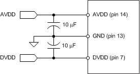 Figure 51. Power-Supply Decoupling