ZHCSJX5 June 2019 ADS7028
ADVANCE INFORMATION for pre-production products; subject to change without notice.
- 1 特性
- 2 应用
- 3 说明
- 4 修订历史记录
- 5 Device Comparison Table
- 6 Pin Configuration and Functions
- 7 Specifications
-
8 Detailed Description
- 8.1 Overview
- 8.2 Functional Block Diagram
- 8.3
Feature Description
- 8.3.1 Multiplexer and ADC
- 8.3.2 Reference
- 8.3.3 ADC Transfer Function
- 8.3.4 ADC Offset Calibration
- 8.3.5 Programmable Averaging Filter
- 8.3.6 CRC on Data Interface
- 8.3.7 General-Purpose I/Os
- 8.3.8 Oscillator and Timing Control
- 8.3.9 Output Data Format
- 8.3.10 Zero-Crossing-Detect Module
- 8.3.11 Digital Window Comparator
- 8.3.12 Root-Mean-Square Module
- 8.3.13 Minimum, Maximum, and Latest Data Registers
- 8.3.14 Device Programming
- 8.4 Device Functional Modes
- 8.5
ADS7028 Registers
- 8.5.1 SYSTEM_STATUS Register (Address = 0x0) [reset = 0x81]
- 8.5.2 GENERAL_CFG Register (Address = 0x1) [reset = 0x0]
- 8.5.3 DATA_CFG Register (Address = 0x2) [reset = 0x0]
- 8.5.4 OSR_CFG Register (Address = 0x3) [reset = 0x0]
- 8.5.5 OPMODE_CFG Register (Address = 0x4) [reset = 0x0]
- 8.5.6 PIN_CFG Register (Address = 0x5) [reset = 0x0]
- 8.5.7 GPIO_CFG Register (Address = 0x7) [reset = 0x0]
- 8.5.8 GPO_DRIVE_CFG Register (Address = 0x9) [reset = 0x0]
- 8.5.9 GPO_OUTPUT_VALUE Register (Address = 0xB) [reset = 0x0]
- 8.5.10 GPI_VALUE Register (Address = 0xD) [reset = 0x0]
- 8.5.11 ZCD_BLANKING_CFG Register (Address = 0xF) [reset = 0x0]
- 8.5.12 SEQUENCE_CFG Register (Address = 0x10) [reset = 0x0]
- 8.5.13 CHANNEL_SEL Register (Address = 0x11) [reset = 0x0]
- 8.5.14 AUTO_SEQ_CH_SEL Register (Address = 0x12) [reset = 0x0]
- 8.5.15 ALERT_CH_SEL Register (Address = 0x14) [reset = 0x0]
- 8.5.16 ALERT_MAP Register (Address = 0x16) [reset = 0x0]
- 8.5.17 ALERT_PIN_CFG Register (Address = 0x17) [reset = 0x0]
- 8.5.18 EVENT_FLAG Register (Address = 0x18) [reset = 0x0]
- 8.5.19 EVENT_HIGH_FLAG Register (Address = 0x1A) [reset = 0x0]
- 8.5.20 EVENT_LOW_FLAG Register (Address = 0x1C) [reset = 0x0]
- 8.5.21 EVENT_RGN Register (Address = 0x1E) [reset = 0x0]
- 8.5.22 HYSTERESIS_CH0 Register (Address = 0x20) [reset = 0xF0]
- 8.5.23 HIGH_TH_CH0 Register (Address = 0x21) [reset = 0xFF]
- 8.5.24 EVENT_COUNT_CH0 Register (Address = 0x22) [reset = 0x0]
- 8.5.25 LOW_TH_CH0 Register (Address = 0x23) [reset = 0x0]
- 8.5.26 HYSTERESIS_CH1 Register (Address = 0x24) [reset = 0xF0]
- 8.5.27 HIGH_TH_CH1 Register (Address = 0x25) [reset = 0xFF]
- 8.5.28 EVENT_COUNT_CH1 Register (Address = 0x26) [reset = 0x0]
- 8.5.29 LOW_TH_CH1 Register (Address = 0x27) [reset = 0x0]
- 8.5.30 HYSTERESIS_CH2 Register (Address = 0x28) [reset = 0xF0]
- 8.5.31 HIGH_TH_CH2 Register (Address = 0x29) [reset = 0xFF]
- 8.5.32 EVENT_COUNT_CH2 Register (Address = 0x2A) [reset = 0x0]
- 8.5.33 LOW_TH_CH2 Register (Address = 0x2B) [reset = 0x0]
- 8.5.34 HYSTERESIS_CH3 Register (Address = 0x2C) [reset = 0xF0]
- 8.5.35 HIGH_TH_CH3 Register (Address = 0x2D) [reset = 0xFF]
- 8.5.36 EVENT_COUNT_CH3 Register (Address = 0x2E) [reset = 0x0]
- 8.5.37 LOW_TH_CH3 Register (Address = 0x2F) [reset = 0x0]
- 8.5.38 HYSTERESIS_CH4 Register (Address = 0x30) [reset = 0xF0]
- 8.5.39 HIGH_TH_CH4 Register (Address = 0x31) [reset = 0xFF]
- 8.5.40 EVENT_COUNT_CH4 Register (Address = 0x32) [reset = 0x0]
- 8.5.41 LOW_TH_CH4 Register (Address = 0x33) [reset = 0x0]
- 8.5.42 HYSTERESIS_CH5 Register (Address = 0x34) [reset = 0xF0]
- 8.5.43 HIGH_TH_CH5 Register (Address = 0x35) [reset = 0xFF]
- 8.5.44 EVENT_COUNT_CH5 Register (Address = 0x36) [reset = 0x0]
- 8.5.45 LOW_TH_CH5 Register (Address = 0x37) [reset = 0x0]
- 8.5.46 HYSTERESIS_CH6 Register (Address = 0x38) [reset = 0xF0]
- 8.5.47 HIGH_TH_CH6 Register (Address = 0x39) [reset = 0xFF]
- 8.5.48 EVENT_COUNT_CH6 Register (Address = 0x3A) [reset = 0x0]
- 8.5.49 LOW_TH_CH6 Register (Address = 0x3B) [reset = 0x0]
- 8.5.50 HYSTERESIS_CH7 Register (Address = 0x3C) [reset = 0xF0]
- 8.5.51 HIGH_TH_CH7 Register (Address = 0x3D) [reset = 0xFF]
- 8.5.52 EVENT_COUNT_CH7 Register (Address = 0x3E) [reset = 0x0]
- 8.5.53 LOW_TH_CH7 Register (Address = 0x3F) [reset = 0x0]
- 8.5.54 MAX_CH0_LSB Register (Address = 0x60) [reset = 0x0]
- 8.5.55 MAX_CH0_MSB Register (Address = 0x61) [reset = 0x0]
- 8.5.56 MAX_CH1_LSB Register (Address = 0x62) [reset = 0x0]
- 8.5.57 MAX_CH1_MSB Register (Address = 0x63) [reset = 0x0]
- 8.5.58 MAX_CH2_LSB Register (Address = 0x64) [reset = 0x0]
- 8.5.59 MAX_CH2_MSB Register (Address = 0x65) [reset = 0x0]
- 8.5.60 MAX_CH3_LSB Register (Address = 0x66) [reset = 0x0]
- 8.5.61 MAX_CH3_MSB Register (Address = 0x67) [reset = 0x0]
- 8.5.62 MAX_CH4_LSB Register (Address = 0x68) [reset = 0x0]
- 8.5.63 MAX_CH4_MSB Register (Address = 0x69) [reset = 0x0]
- 8.5.64 MAX_CH5_LSB Register (Address = 0x6A) [reset = 0x0]
- 8.5.65 MAX_CH5_MSB Register (Address = 0x6B) [reset = 0x0]
- 8.5.66 MAX_CH6_LSB Register (Address = 0x6C) [reset = 0x0]
- 8.5.67 MAX_CH6_MSB Register (Address = 0x6D) [reset = 0x0]
- 8.5.68 MAX_CH7_LSB Register (Address = 0x6E) [reset = 0x0]
- 8.5.69 MAX_CH7_MSB Register (Address = 0x6F) [reset = 0x0]
- 8.5.70 MIN_CH0_LSB Register (Address = 0x80) [reset = 0xFF]
- 8.5.71 MIN_CH0_MSB Register (Address = 0x81) [reset = 0xFF]
- 8.5.72 MIN_CH1_LSB Register (Address = 0x82) [reset = 0xFF]
- 8.5.73 MIN_CH1_MSB Register (Address = 0x83) [reset = 0xFF]
- 8.5.74 MIN_CH2_LSB Register (Address = 0x84) [reset = 0xFF]
- 8.5.75 MIN_CH2_MSB Register (Address = 0x85) [reset = 0xFF]
- 8.5.76 MIN_CH3_LSB Register (Address = 0x86) [reset = 0xFF]
- 8.5.77 MIN_CH3_MSB Register (Address = 0x87) [reset = 0xFF]
- 8.5.78 MIN_CH4_LSB Register (Address = 0x88) [reset = 0xFF]
- 8.5.79 MIN_CH4_MSB Register (Address = 0x89) [reset = 0xFF]
- 8.5.80 MIN_CH5_LSB Register (Address = 0x8A) [reset = 0xFF]
- 8.5.81 MIN_CH5_MSB Register (Address = 0x8B) [reset = 0xFF]
- 8.5.82 MIN_CH6_LSB Register (Address = 0x8C) [reset = 0xFF]
- 8.5.83 MIN_CH6_MSB Register (Address = 0x8D) [reset = 0xFF]
- 8.5.84 MIN_CH7_LSB Register (Address = 0x8E) [reset = 0xFF]
- 8.5.85 MIN_CH7_MSB Register (Address = 0x8F) [reset = 0xFF]
- 8.5.86 RECENT_CH0_LSB Register (Address = 0xA0) [reset = 0x0]
- 8.5.87 RECENT_CH0_MSB Register (Address = 0xA1) [reset = 0x0]
- 8.5.88 RECENT_CH1_LSB Register (Address = 0xA2) [reset = 0x0]
- 8.5.89 RECENT_CH1_MSB Register (Address = 0xA3) [reset = 0x0]
- 8.5.90 RECENT_CH2_LSB Register (Address = 0xA4) [reset = 0x0]
- 8.5.91 RECENT_CH2_MSB Register (Address = 0xA5) [reset = 0x0]
- 8.5.92 RECENT_CH3_LSB Register (Address = 0xA6) [reset = 0x0]
- 8.5.93 RECENT_CH3_MSB Register (Address = 0xA7) [reset = 0x0]
- 8.5.94 RECENT_CH4_LSB Register (Address = 0xA8) [reset = 0x0]
- 8.5.95 RECENT_CH4_MSB Register (Address = 0xA9) [reset = 0x0]
- 8.5.96 RECENT_CH5_LSB Register (Address = 0xAA) [reset = 0x0]
- 8.5.97 RECENT_CH5_MSB Register (Address = 0xAB) [reset = 0x0]
- 8.5.98 RECENT_CH6_LSB Register (Address = 0xAC) [reset = 0x0]
- 8.5.99 RECENT_CH6_MSB Register (Address = 0xAD) [reset = 0x0]
- 8.5.100 RECENT_CH7_LSB Register (Address = 0xAE) [reset = 0x0]
- 8.5.101 RECENT_CH7_MSB Register (Address = 0xAF) [reset = 0x0]
- 8.5.102 RMS_CFG Register (Address = 0xC0) [reset = 0x0]
- 8.5.103 RMS_LSB Register (Address = 0xC1) [reset = 0x0]
- 8.5.104 RMS_MSB Register (Address = 0xC2) [reset = 0x0]
- 8.5.105 GPO0_TRIG_EVENT_SEL Register (Address = 0xC3) [reset = 0x2]
- 8.5.106 GPO1_TRIG_EVENT_SEL Register (Address = 0xC5) [reset = 0x1]
- 8.5.107 GPO2_TRIG_EVENT_SEL Register (Address = 0xC7) [reset = 0x8]
- 8.5.108 GPO3_TRIG_EVENT_SEL Register (Address = 0xC9) [reset = 0x4]
- 8.5.109 GPO4_TRIG_EVENT_SEL Register (Address = 0xCB) [reset = 0x20]
- 8.5.110 GPO5_TRIG_EVENT_SEL Register (Address = 0xCD) [reset = 0x10]
- 8.5.111 GPO6_TRIG_EVENT_SEL Register (Address = 0xCF) [reset = 0x80]
- 8.5.112 GPO7_TRIG_EVENT_SEL Register (Address = 0xD1) [reset = 0x40]
- 8.5.113 GPO_VALUE_ZCD_CFG_CH0_CH3 Register (Address = 0xE3) [reset = 0x0]
- 8.5.114 GPO_VALUE_ZCD_CFG_CH4_CH7 Register (Address = 0xE4) [reset = 0x0]
- 8.5.115 GPO_ZCD_UPDATE_EN Register (Address = 0xE7) [reset = 0x0]
- 8.5.116 GPO_TRIGGER_CFG Register (Address = 0xE9) [reset = 0x0]
- 8.5.117 GPO_VALUE_TRIG Register (Address = 0xEB) [reset = 0x0]
- 9 Application and Implementation
- 10Power Supply Recommendations
- 11Layout
- 12器件和文档支持
- 13机械、封装和可订购信息
7.7 Switching Characteristics
at AVDD = 5 V, DVDD = 1.65 V to 5.5 V, and maximum throughput (unless otherwise noted); minimum and maximum values at TA = –40°C to +85°C; typical values at TA = 25°C| PARAMETER | Test Conditions | MIN | MAX | UNIT | |
|---|---|---|---|---|---|
| CONVERSION CYCLE | |||||
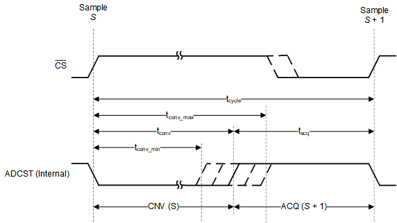
| tCONV | ADC conversion time | 600 | ns | ||
| tACQ | Acquisition time | 400 | ns | ||
| RESET and ALERT | |||||
| tPU | Power-up time for device | AVDD ≥ 2.35 V, CDECAP = 1 µF | 5 | ms | |
| tRST | Delay time; RST bit = 1b to device reset complete(1) | 5 | ms | ||
| tALERT_HI | ALERT high period | ALERT_LOGIC[1:0] = 1x | 85 | 105 | ns |
| tALERT_LO | ALERT low period | ALERT_LOGIC[1:0] = 1x | 85 | 105 | ns |
| SPI INTERFACE TIMINGS | |||||
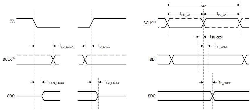
| tDEN_CSDO | Delay time: CS falling to data enable | 15 | ns | ||
| tDZ_CSDO | Delay time: CS rising to SDO going Hi-Z | 15 | ns | ||
| tD_CKDO | Delay time: SCLK launch edge to (next) data valid on SDO | 15 | ns | ||
 Figure 1. Conversion Cycle Timing
1. The SCLK polarity, launch edge, and capture edge depend on the SPI protocol selected.
Figure 2. SPI-Compatible Serial Interface Timing