ZHCSFP3C August 2016 – June 2017 ADS124S06 , ADS124S08
PRODUCTION DATA.
- 1 特性
- 2 应用
- 3 说明
- 4 修订历史记录
- 5 Device Family Comparison Table
- 6 Pin Configuration and Functions
- 7 Specifications
- 8 Parameter Measurement Information
-
9 Detailed Description
- 9.1 Overview
- 9.2 Functional Block Diagram
- 9.3
Feature Description
- 9.3.1 Multiplexer
- 9.3.2 Low-Noise Programmable Gain Amplifier
- 9.3.3 Voltage Reference
- 9.3.4 Clock Source
- 9.3.5 Delta-Sigma Modulator
- 9.3.6 Digital Filter
- 9.3.7 Excitation Current Sources (IDACs)
- 9.3.8 Bias Voltage Generation
- 9.3.9 System Monitor
- 9.3.10 Status Register
- 9.3.11 General-Purpose Inputs and Outputs (GPIOs)
- 9.3.12 Low-Side Power Switch
- 9.3.13 Cyclic Redundancy Check (CRC)
- 9.3.14 Calibration
- 9.4 Device Functional Modes
- 9.5 Programming
- 9.6
Register Map
- 9.6.1
Configuration Registers
- 9.6.1.1 Device ID Register (address = 00h) [reset = xxh]
- 9.6.1.2 Device Status Register (address = 01h) [reset = 80h]
- 9.6.1.3 Input Multiplexer Register (address = 02h) [reset = 01h]
- 9.6.1.4 Gain Setting Register (address = 03h) [reset = 00h]
- 9.6.1.5 Data Rate Register (address = 04h) [reset = 14h]
- 9.6.1.6 Reference Control Register (address = 05h) [reset = 10h]
- 9.6.1.7 Excitation Current Register 1 (address = 06h) [reset = 00h]
- 9.6.1.8 Excitation Current Register 2 (address = 07h) [reset = FFh]
- 9.6.1.9 Sensor Biasing Register (address = 08h) [reset = 00h]
- 9.6.1.10 System Control Register (address = 09h) [reset = 10h]
- 9.6.1.11 Offset Calibration Register 1 (address = 0Ah) [reset = 00h]
- 9.6.1.12 Offset Calibration Register 2 (address = 0Bh) [reset = 00h]
- 9.6.1.13 Offset Calibration Register 3 (address = 0Ch) [reset = 00h]
- 9.6.1.14 Gain Calibration Register 1 (address = 0Dh) [reset = 00h]
- 9.6.1.15 Gain Calibration Register 2 (address = 0Eh) [reset = 00h]
- 9.6.1.16 Gain Calibration Register 3 (address = 0Fh) [reset = 40h]
- 9.6.1.17 GPIO Data Register (address = 10h) [reset = 00h]
- 9.6.1.18 GPIO Configuration Register (address = 11h) [reset = 00h]
- 9.6.1
Configuration Registers
- 10Application and Implementation
- 11Power Supply Recommendations
- 12Layout
- 13器件和文档支持
- 14机械、封装和可订购信息
封装选项
机械数据 (封装 | 引脚)
散热焊盘机械数据 (封装 | 引脚)
订购信息
10 Application and Implementation
NOTE
Information in the following applications sections is not part of the TI component specification, and TI does not warrant its accuracy or completeness. TI’s customers are responsible for determining suitability of components for their purposes. Customers should validate and test their design implementation to confirm system functionality.
10.1 Application Information
The ADS124S06 and ADS124S08 are precision, 24-bit, ΔΣ ADCs that offer many integrated features to simplify the measurement of the most common sensor types (including various types of temperature, flow, and bridge sensors). Primary considerations when designing an application with the ADS124S0x include analog input filtering, establishing an appropriate reference, and setting the absolute input voltage for the internal PGA. Connecting and configuring the serial interface appropriately is another concern. These considerations are discussed in the following sections.
10.1.1 Serial Interface Connections
The principle serial interface connections for the ADS124S0x are shown in Figure 111.
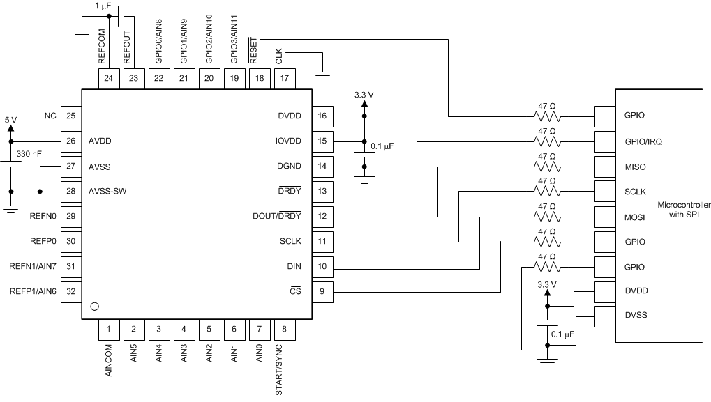 Figure 111. Serial Interface Connections
Most microcontroller SPI peripherals can interface with the ADS124S0x. The interface operates in SPI mode 1 where CPOL = 0 and CPHA = 1. In SPI mode 1, SCLK idles low and data are launched or changed only on SCLK rising edges; data are latched or read by the master and slave on SCLK falling edges. Details of the SPI communication protocol employed by the devices are found in the Serial Interface section.
Place 47-Ω resistors in series with all digital input and output pins (CS, SCLK, DIN, DOUT/DRDY, and DRDY). This resistance smooths sharp transitions, suppresses overshoot, and offers some overvoltage protection. Care must be taken to meet all SPI timing requirements because the additional resistors interact with the bus capacitances present on the digital signal lines.
10.1.2 Analog Input Filtering
Analog input filtering serves two purposes: first, to limit the effect of aliasing during the sampling process and second, to reduce external noise from being a part of the measurement.
As with any sampled system, aliasing can occur if proper antialias filtering is not in place. Aliasing occurs when frequency components are present in the input signal that are higher than half the sampling frequency of the ADC (also known as the Nyquist frequency). These frequency components are folded back and show up in the actual frequency band of interest below half the sampling frequency. Note that inside a ΔΣ ADC, the input signal is oversampled at the modulator frequency, fMOD and not at the output data rate. The filter response of the digital filter repeats at multiples of fMOD, as shown in Figure 112. Signals or noise up to a frequency where the filter response repeats are attenuated to a certain amount by the digital filter depending on the filter architecture. Any frequency components present in the input signal around the modulator frequency or multiples thereof are not attenuated and alias back into the band of interest, unless attenuated by an external analog filter.
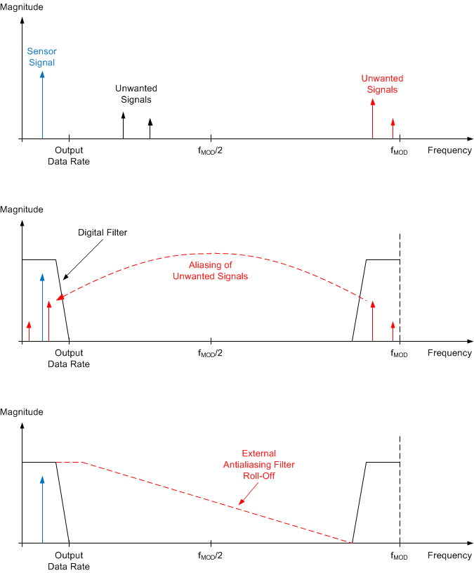 Figure 112. Effect of Aliasing
Many sensor signals are inherently band limited; for example, the output of a thermocouple has a limited rate of change. In this case, the sensor signal does not alias back into the pass band when using a ΔΣ ADC. However, any noise pick-up along the sensor wiring or the application circuitry can potentially alias into the pass band. Power line-cycle frequency and harmonics are one common noise source. External noise can also be generated from electromagnetic interference (EMI) or radio frequency interference (RFI) sources, such as nearby motors and cellular phones. Another noise source typically exists on the printed circuit board (PCB) itself in the form of clocks and other digital signals. Analog input filtering helps remove unwanted signals from affecting the measurement result.
A first-order resistor-capacitor (RC) filter is (in most cases) sufficient to either eliminate aliasing, or to reduce the effect of aliasing to a level below the noise floor of the sensor. Ideally, any signal beyond fMOD / 2 is attenuated to a level below the noise floor of the ADC. The digital filter of the ADS124S0x attenuates signals to a certain degree, as illustrated in the filter response plots in the Digital Filter section. In addition, noise components are usually smaller in magnitude than the actual sensor signal. Therefore, using a first-order RC filter with a cutoff frequency set at the output data rate or 10 times higher is generally a good starting point for a system design.
Internal to the device, prior to the PGA inputs, is an EMI filter; see Figure 50. The cutoff frequency of this filter is approximately 40 MHz and helps reject high-frequency interference.
10.1.3 External Reference and Ratiometric Measurements
The full-scale range of the ADS124S0x is defined by the reference voltage and the PGA gain
(FSR = ±VREF / Gain). An external reference can be used instead of the integrated 2.5-V reference to adapt the FSR to the specific system needs. An external reference must be used if VIN > 2.5 V. For example, an external
5-V reference and an AVDD = 5 V are required in order to measure a single-ended signal that can swing between 0 V and 5 V.
The reference inputs of the device also allow the implementation of ratiometric measurements. In a ratiometric measurement, the same excitation source that is used to excite the sensor is also used to establish the reference for the ADC. As an example, a simple form of a ratiometric measurement uses the same current source to excite both the resistive sensor element (such as an RTD) and another resistive reference element that is in series with the element being measured. The voltage that develops across the reference element is used as the reference source for the ADC. Because current noise and drift are common to both the sensor measurement and the reference, these components cancel out in the ADC transfer function. The output code is only a ratio of the sensor element and the value of the reference resistor. The value of the excitation current source itself is not part of the ADC transfer function.
The example in the Typical Application section describes a system that uses a ratiometric measurement. One excitation current source is used to drive a reference resistor and an RTD. The ADC measurement represents a ratiometric measurement between the RTD value and a known reference resistor value.
10.1.4 Establishing a Proper Input Voltage
The ADS124S0x can be used to measure various types of input signal configurations: single-ended, pseudo-differential, and fully-differential signals (which can be either unipolar or bipolar). However, configuring the device properly for the respective signal type is important.
Signals where the negative analog input is fixed and referenced to analog ground (VAINN = 0 V) are commonly called single-ended signals. The input voltage of a single-ended signal consequently varies between 0 V and VIN. If the PGA is disabled and bypassed, the input voltage of the ADS124S08 can be as low as 50 mV below AVSS and as large as 50 mV above AVDD. Therefore, set the PGA_EN bits to 10 in the gain setting register (03h) to measure single-ended signals when a unipolar analog supply is used (AVSS = 0 V). Only a gain of 1 is possible in this configuration. Measuring a 0-mA to 20-mA or 4-mA to 20-mA signal across a load resistor of 100 Ω referenced to GND is a typical example. The ADS124S0x can directly measure the signal across the load resistor using a unipolar supply, the internal 2.5-V reference, and gain = 1 when the PGA is bypassed.
If gain is needed to measure a single-ended signal, the PGA must be enabled. In this case, a bipolar supply is required for the ADS124S0x to meet the input voltage requirement of the PGA. Signals where the negative analog input (AINN) is fixed at a voltage other the 0 V are referred to as pseudo-differential signals. The input voltage of a pseudo-differential signal varies between VAINN and VAINN + VIN.
Fully-differential signals in contrast are defined as signals having a constant common-mode voltage where the positive and negative analog inputs swing 180° out-of-phase but have the same amplitude.
The ADS124S0x can measure pseudo-differential and fully-differential signals both with the PGA enabled or bypassed. However, the PGA must be enabled in order to measure any input with a gain greater than 1. The input voltage must meet the input and output voltage restrictions of the PGA, as explained in the PGA Input-Voltage Requirements section when the PGA is enabled. Setting the input voltage at or near (AVSS + AVDD) / 2 in most cases satisfies the PGA input voltage requirements.
Signals where both the positive and negative inputs are always ≥ 0 V are called unipolar signals. These signals can in general be measured with the ADS124S0x using a unipolar analog supply (AVSS = 0 V). As mentioned previously, the PGA must be bypassed in order to measure single-ended, unipolar signals when using a unipolar supply.
A signal is called bipolar when either the positive or negative input can swing below 0 V. A bipolar analog supply (such as AVDD = 2.5 V, AVSS = –2.5 V) is required in order to measure bipolar signals with the ADS124S0x. A typical application task is measuring a single-ended, bipolar, ±10-V signal where AINN is fixed at 0 V and AINP swings between –10 V and 10 V. The ADS124S0x cannot directly measure this signal because the 10-V signal exceeds the analog power-supply limits. However, one possible solution is to use a bipolar analog supply (AVDD = 2.5 V, AVSS = –2.5 V), gain = 1, and a resistor divider in front of the ADS124S0x. The resistor divider must divide the voltage down to ≤ ±2.5 V to be able to measure the voltage using the internal 2.5-V reference.
10.1.5 Unused Inputs and Outputs
To minimize leakage currents on the analog inputs, leave unused analog and reference inputs floating, or connect the inputs to mid-supply or to AVDD. Connecting unused analog or reference inputs to AVSS is possible as well, but can yield higher leakage currents than the previously mentioned options. REFN0 is an exception; this pin can be accidently shorted to AVSS through the internal low-side switch. Leave the REFN0 pin floating when not in use or tie the pin to AVSS.
GPIO pins operate on levels based on the analog supply. Do not float GPIO pins that are configured as digital inputs. Tie unused GPIO pins that are configured as digital inputs to the appropriate levels, AVDD or AVSS, including when in power-down mode. Tie unused GPIO output pins to AVSS through a pulldown resistor and set the output to 0 in the GPIO data register. For unused GPIO pins on the ADS124S06, leave the GPIOCON register set to the default register values and connect these GPIO pins in the same manner as for an unused analog input.
Do not float unused digital inputs; excessive power-supply leakage current can result. Tie all unused digital inputs to the appropriate levels, IOVDD or DGND, even when in power-down mode. Connections for unused digital inputs are listed below.
- Tie the CS pin to DGND if CS is not used
- Tie the CLK pin to DGND if the internal oscillator is used
- Tie the START/SYNC pin to DGND to control conversions by commands
- Tie the RESET pin to IOVDD if the RESET pin is not used
- If the DRDY output is not used, leave the DRDY pin unconnected or tie the DRDY pin to IOVDD using a weak pullup resistor
10.1.6 Pseudo Code Example
The following list shows a pseudo code sequence with the required steps to set up the device and the microcontroller that interfaces to the ADC in order to take subsequent readings from the ADS124S0x in continuous conversion mode. The dedicated DRDY pin is used to indicate availability of new conversion data.
Power-up so that all supplies reach minimum operating levels;
Delay for a minimum of 2.2 ms to allow power supplies to settle and power-up reset to complete;

Configure the SPI interface of the microcontroller to SPI mode 1 (CPOL = 0, CPHA =1);
If the CS pin is not tied low permanently, configure the microcontroller GPIO connected to CS as an
output;
Configure the microcontroller GPIO connected to the DRDY pin as a falling edge triggered interrupt
input;

Set CS to the device low;
Delay for a minimum of td(CSSC);
Send the RESET command (06h) to make sure the device is properly reset after power-up; //Optional
Delay for a minimum of 4096 · tCLK;
Read the status register using the RREG command to check that the RDY bit is 0; //Optional
Clear the FL_POR flag by writing 00h to the status register; //Optional
Write the respective register configuration with the WREG command;
For verification, read back all configuration registers with the RREG command;
Send the START command (08h) to start converting in continuous conversion mode;
Delay for a minimum of td(SCCS);
Clear CS to high (resets the serial interface);
Loop
	{
	Wait for DRDY to transition low;
	Take CS low;
	Delay for a minimum of td(CSSC);
 Send the RDATA command;
	Send 24 SCLK rising edges to read out conversion data on DOUT/DRDY;
	Delay for a minimum of td(SCCS);
	Clear CS to high;
	}
Take CS low;
Delay for a minimum of td(CSSC);
Send the STOP command (0Ah) to stop conversions and put the device in standby mode;
Delay for a minimum of td(SCCS);
Clear CS to high;
10.2 Typical Application
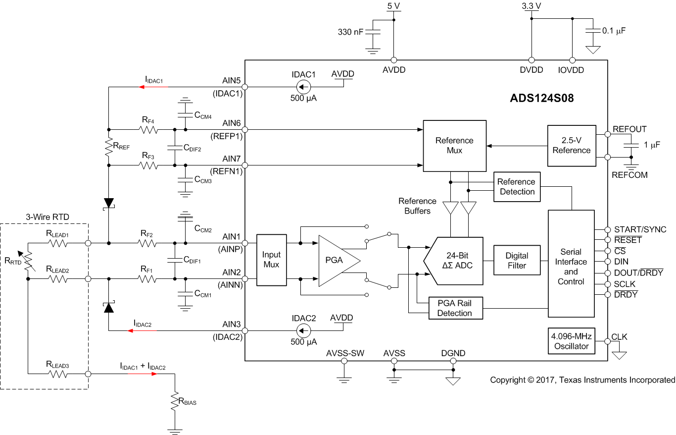
Figure 113 shows a fault-protected, filtered, 3-wire RTD application circuit with hardware-based, lead-wire compensation. Two IDAC current sources provide the lead-wire compensation. One IDAC current source (IDAC1) provides excitation to the RTD element. The ADC reference voltage (pins AIN6 and AIN7) is derived from the voltage across resistor RREF sourcing the same IDAC1 current, providing ratiometric cancellation of current-source drift. The other current source (IDAC2) has the same current setting, providing cancellation of lead-wire resistance by generating a voltage drop across lead-wire resistance RLEAD2 equal to the voltage drop of RLEAD1. Because the RRTD voltage is measured differentially at ADC pins AIN1 and AIN2, the voltages across the lead wire resistance cancel. Resistor RBIAS level-shifts the RTD signal to within the ADC specified input range. The current sources are provided by two additional pins (AIN5 and AIN3) that connect to the RTD through blocking diodes. The additional pins are used to route the RTD excitation currents around the input filter resistors, avoiding the voltage drop otherwise caused by the filter resistors RF1 and RF4. The diodes protect the ADC inputs in the event of a miswired connection. The input filter resistors limit the input fault currents flowing into the ADC.
10.2.1 Design Requirements
Table 44 shows the design requirements of the 3-wire RTD application.
Table 44. Design Requirements
| DESIGN PARAMETER | VALUE |
|---|---|
| ADC supply voltage | 4.75 V (minimum) |
| RTD sensor type | 3-wire Pt100 |
| RTD resistance range | 20 Ω to 400 Ω |
| RTD lead resistance range | 0 Ω to 10 Ω |
| RTD self heating | 1 mW |
| Accuracy(1) | ±0.05 Ω |
10.2.2 Detailed Design Procedure
The key considerations in the design of a 3-wire RTD circuit are the accuracy, the lead wire compensation, and the sensor self-heating. As the design values of Table 45 show, several values of excitation currents are available. The resolution is expressed in units of noise-free resolution (NFR). Noise-free resolution is resolution with no code flicker. The selection of excitation currents trades off resolution against sensor self-heating. In general, measurement resolution improves with increasing excitation current. Increasing the excitation current beyond 1000 µA results in no further improvement in resolution for this example circuit. The design procedure is based on a 500-µA excitation current, because this level of current results in very low sensor self-heating
(0.4 mW).
Table 45. RTD Circuit Design Parameters
| IIDAC (µA) | NFR (bits) | PRTD (mW) | VRTD
(V) |
Gain
(V/V) |
VREFMIN(1)
(V) |
VREF(2)
(V) |
RREF
(kΩ) |
VAINNLIM(3)
(V) |
VAINPLIM(4)
(V) |
RBIAS
(kΩ) |
VRTDN(5)
(V) |
VRTDP(6)
(V) |
VIDAC1(7)
(V) |
|---|---|---|---|---|---|---|---|---|---|---|---|---|---|
| 50 | 16.8 | 0.001 | 0.02 | 32 | 0.64 | 0.70 | 18 | 0.6 | 4.1 | 7.10 | 0.7 | 0.7 | 1.9 |
| 100 | 17.8 | 0.004 | 0.04 | 32 | 1.28 | 1.41 | 14.1 | 0.9 | 3.8 | 5.10 | 1.0 | 1.1 | 2.8 |
| 250 | 18.8 | 0.025 | 0.10 | 16 | 1.60 | 1.76 | 7.04 | 1.1 | 3.7 | 2.30 | 1.2 | 1.3 | 3.3 |
| 500 | 19.1 | 0.100 | 0.20 | 8 | 1.60 | 1.76 | 3.52 | 1.0 | 3.8 | 1.10 | 1.1 | 1.3 | 3.4 |
| 750 | 18.9 | 0.225 | 0.30 | 4 | 1.20 | 1.32 | 1.76 | 0.8 | 4.0 | 0.57 | 0.9 | 1.2 | 2.8 |
| 1000 | 19.3 | 0.400 | 0.40 | 4 | 1.60 | 1.76 | 1.76 | 0.9 | 3.9 | 0.50 | 1.0 | 1.4 | 3.5 |
| 1500 | 19.1 | 0.900 | 0.60 | 2 | 1.20 | 1.32 | 0.88 | 0.6 | 4.2 | 0.23 | 0.7 | 1.3 | 3.0 |
| 2000 | 18.3 | 1.600 | 0.80 | 1 | 0.80 | 0.90 | 0.45 | 0.3 | 4.5 | 0.10 | 0.4 | 1.2 | 2.4 |
Initially, RLEAD1 and RLEAD2 are considered to be 0 Ω. Route the IDAC1 current through the external reference resistor, RREF. IDAC1 generates the ADC reference voltage, VREF, across the reference resistor. This voltage is defined by Equation 12:
Route the second current (IDAC2) to the second RTD lead.
Program the IDAC value by using the IDACMAG register; however, only the IDAC1 current flows through the reference resistor and RTD. The IDAC1 current excites the RTD to produce a voltage proportional to the RTD resistance. The RTD voltage is defined by Equation 13:
The ADC amplifies the RTD signal voltage (VRTD) and measures the resulting voltage against the reference voltage to produce a proportional digital output code, as shown in Equation 14 through Equation 16.
As shown in Equation 16, the RTD measurement depends on the value of the RTD, the PGA gain, and the reference resistor RREF, but not on the IDAC1 value. Therefore, the absolute accuracy and temperature drift of the excitation current does not matter.
The second excitation current (IDAC2) provides a second voltage drop across the second RTD lead resistance, RLEAD2. The second voltage drop compensates the voltage drop caused by IDAC1 and RLEAD1. The leads of a 3-wire RTD typically have the same length; therefore, the lead resistance is typically identical. Taking the lead resistance into account (RLEADx ≠ 0), the differential voltage (VIN) across ADC inputs AIN8 and AIN9 is shown in Equation 17:
If RLEAD1 = RLEAD2 and IIDAC1 = IIDAC2, the expression for VIN reduces to Equation 18:
In other words, the measurement error resulting from the voltage drop across the RTD lead resistance is compensated as long as the lead resistance values and the IDAC values are matched.
Using Equation 13, the value of RTD resistance (400 Ω, maximum) and the excitation current (500 µA) yields an RTD voltage of VRTD = 500 µA · 400 Ω = 0.2 V. Use the maximum gain of 8 in order to limit the corresponding loop voltage of IDAC1. Gain = 8 requires a minimum reference voltage VREFMIN = 0.2 V · 8 = 1.6 V. To provide margin for the ADC operating range, increase the target reference voltage by 10% (VREF = 1.6 V · 1.1 = 1.76 V). Calculate the value of the reference resistor, as shown in Equation 19:
For this example application, 3.5 kΩ is chosen for RREF. For best results, use a precision reference resistor RREF with a low temperature drift (< 10 ppm/°C). Any change in RREF is reflected in the measurement as a gain error.
The next step in the design is determining the value of the RBIAS resistor, in order to level shift the RTD voltage to meet the ADC absolute input-voltage specification. The required level-shift voltage is determined by calculating the minimum absolute voltage (VAINNLIM) as shown in Equation 20:
where
- VRTDMAX = maximum differential RTD voltage = 0.2 V
- Gain = 8
- AVSS = 0 V
The result of the equation requires a minimum absolute input voltage (VRTDN) > 0.85 V. Therefore, the RTD voltage must be level shifted by a minimum of 0.85 V. To meet this requirement, a target level-shift value of 1 V is chosen to provide extra margin. Calculate the value of RBIAS as shown in Equation 21:
After the level-shift voltage is determined, verify that the positive RTD voltage (VRTDP) is less than the maximum absolute input voltage (VAINPLIM), as shown in Equation 22:
where
- VRTDMAX = maximum differential RTD voltage = 0.2 V
- Gain = 8
- AVDD = 4.75 V (minimum)
Solving Equation 22 results in a required VRTDP of less than 3.9 V. Calculate the VRTDP input voltage by Equation 23:
Because 1.2 V is less than the 3.9-V maximum input voltage limit, the absolute positive and negative RTD voltages are within the ADC specified input range.
The next step in the design is to verify that the IDACs have enough voltage headroom (compliance voltage) to operate. The loop voltage of the excitation current must be less than the supply voltage minus the specified IDAC compliance voltage. Calculate the voltage drop developed across each IDAC current path to AVSS. In this circuit, IDAC1 has the largest voltage drop developed across its current path. The IDAC1 calculation is sufficient to satisfy IDAC2 because the IDAC2 voltage drop is always less than IDAC1 voltage drop. The sum of voltages in the IDAC1 loop is shown in Equation 24:
where
- VD = external blocking diode voltage
The equation results in a loop voltage of VIDAC1 = 3.0 V. The worst-case current source compliance voltage is: (AVDD – 0.4 V) = (4.75 V – 0.4 V) = 4.35 V. The VIDAC1 loop voltage is less than the specified current source compliance voltage (3.0 V < 4.35 V).
Many applications benefit from using an analog filter at the inputs to remove noise and interference from the signal. Filter components are placed on the ADC inputs (RF1, RF2, CDIF1, CCM1, and CCM2), as well as on the reference inputs (RF3, RF4, CDIF2, CCM3, and CCM4). The filters remove both differential and common-mode noise. The application shows a differential input noise filter formed by RF1, RF2 and CDIF1, with additional differential mode capacitance provided by the common-mode filter capacitors, CCM1 and CCM2. Calculate the differential
–3-dB cutoff frequency as shown in Equation 25:
The common-mode noise filter is formed by components RF1, RF2, CCM1, and CCM2. Calculate the common-mode signal –3-dB cutoff frequency, as shown in Equation 26:
Mismatches in the common-mode filter components convert common-mode noise into differential noise. To reduce the effect of mismatch, use a differential mode filter with a corner frequency that is at least 10 times lower than the common-mode filter corner frequency. The low-frequency differential filter removes the common-mode converted noise. The filter resistors (RFx) also serve as current-limiting resistors. These resistors limit the current into the analog inputs (AINx) of the device to safe levels when an overvoltage occurs on the inputs.
Filter resistors lead to an offset voltage error due to the dc input current leakage flowing into and out of the device. Remove this voltage error by system offset calibration. Resistor values that are too large generate excess thermal noise and degrade the overall noise performance. The recommended range of the filter resistor values is 100 Ω to 10 kΩ. The properties of the capacitors are important because the capacitors are connected to the signal; use high-quality C0G ceramics or film-type capacitors.
For consistent noise performance across the full range of RTD measurements, match the corner frequencies of the input and reference filter. See the RTD Ratiometric Measurements and Filtering Using the ADS1148 and ADS1248 Application Report (SBAA201) for detailed information on matching the input and reference filter.
10.2.2.1 Register Settings
The register settings for this design are shown in Table 46.
Table 46. Register Settings
| REGISTER | NAME | SETTING | DESCRIPTION |
|---|---|---|---|
| 02h | INPMUX | 12h | Select AINP = AIN1 and AINN = AIN2 |
| 03h | PGA | 0Bh | PGA enabled, PGA Gain = 8 |
| 04h | DATARATE | 14h | Continuous conversion mode, low-latency filter, 20-SPS data rate |
| 05h | REF | 06h | Positive and negative reference buffers enabled, REFP1 and REFN1 reference inputs selected, internal reference always on |
| 06h | IDACMAG | 05h | IDAC magnitude set to 500 µA |
| 07h | IDACMUX | 35h | IDAC2 set to AIN3, IDAC1 set to AIN5 |
| 08h | VBIAS | 00h | |
| 09h | SYS | 10h | |
| 0Ah | OFCAL0(1) | xxh | |
| 0Bh | OFCAL1 | xxh | |
| 0Ch | OFCAL2 | xxh | |
| 0Dh | FSCAL0(1) | xxh | |
| 0Eh | FSCAL1 | xxh | |
| 0Fh | FSCAL2 | xxh | |
| 10h | GPIODAT | 00h | |
| 11h | GPIOCON | 00h |
10.2.3 Application Curves
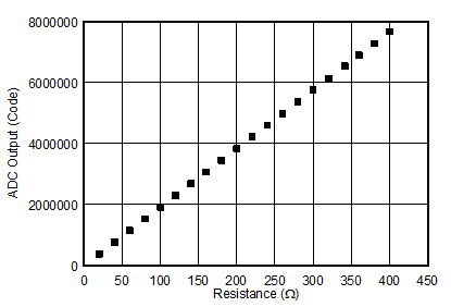
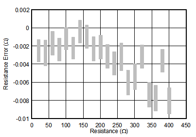
To test the accuracy of the acquisition circuit, a series of calibrated high-precision discrete resistors are used as an input to the system. Measurements are taken at TA = 25°C. Figure 114 displays the resistance measurement over an input span from 20 Ω to 400 Ω. Any offset error is generally attributed to the offset of the ADC, and the gain error can be attributed to the accuracy of the RREF resistor and the ADC. The RREF value is also calibrated to reduce the gain error contribution.
Precision temperature measurement applications are typically calibrated to remove the effects of gain and offset errors that generally dominate the total system error. The simplest calibration method is a linear, or two-point calibration that applies an equal and opposite gain and offset term to cancel the measured system gain and offset error. In this particular tested application, the gain and offset error was very small, and did not require additional calibration other than the self offset and gain calibration provided by the device. The resulting measured resistance error is shown in Figure 115.
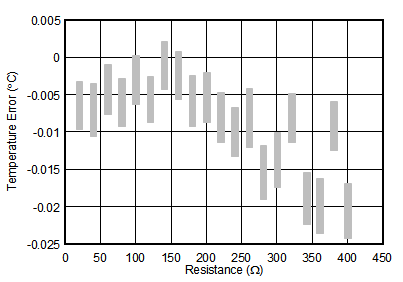
The results in Figure 115 are converted to temperature accuracy by dividing the results by the RTD sensitivity (α) at the measured resistance. Over the full resistance input range, the maximum total measured error is ±0.00929 Ω. Equation 27 uses the measured resistance error and the RTD sensitivity at 0°C to calculate the measured temperature accuracy.
Figure 116 displays the calculated temperature accuracy of the circuit assuming a linear RTD resistance to temperature response. This figure does not include any linearity compensation of the RTD.
10.3 Do's and Don'ts
- Do partition the analog, digital, and power-supply circuitry into separate sections on the PCB.
- Do use a single ground plane for analog and digital grounds.
- Do place the analog components close to the ADC pins using short, direct connections.
- Do keep the SCLK pin free of glitches and noise.
- Do verify that the analog input voltages are within the specified PGA input voltage range under all input conditions.
- Do float unused analog input pins to minimize input leakage current on all other analog inputs. Connecting unused pins to AVDD is the next best option.
- Do provide current limiting to the analog inputs in case overvoltage faults occur.
- Do use a low-dropout linear regulator (LDO) to reduce ripple voltage generated by switch-mode power supplies. Reducing ripple is especially important for AVDD where the supply noise can affect the performance.
- Don't cross analog and digital signals.
- Don't allow the analog and digital power supply voltages to exceed 5.5 V under any condition, including during power-up and power-down.
Figure 117 shows the do's and don'ts of the ADC circuit connections.
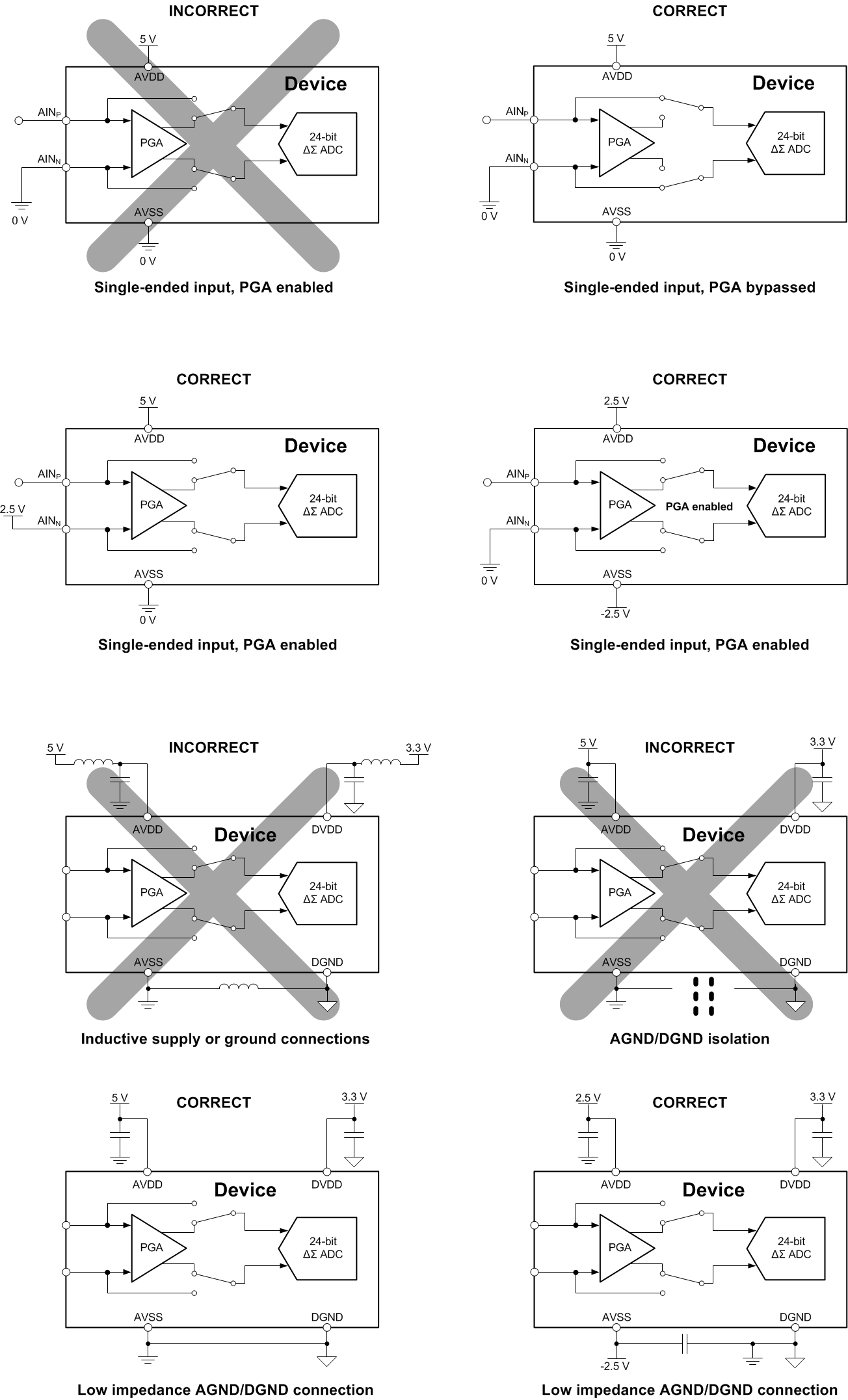 Figure 117. Do's and Don'ts Circuit Connections
