ZHCSIU3 September   2018 ADS1235

PRODUCTION DATA.  

  1. 特性
  2. 应用
  3. 说明
    1.     Device Images
      1.      框图
      2.      ADC 转换噪声
  4. 修订历史记录
  5. Pin Configuration and Functions
    1.     Pin Functions
  6. Specifications
    1. 6.1 Absolute Maximum Ratings
    2. 6.2 ESD Ratings
    3. 6.3 Recommended Operating Conditions
    4. 6.4 Thermal Information
    5. 6.5 Electrical Characteristics
    6. 6.6 Timing Requirements
    7. 6.7 Switching Characteristics
    8. 6.8 Typical Characteristics
  7. Parameter Measurement Information
    1. 7.1 Noise Performance
  8. Detailed Description
    1. 8.1 Overview
    2. 8.2 Functional Block Diagram
    3. 8.3 Feature Description
      1. 8.3.1 Analog Inputs
        1. 8.3.1.1 ESD Diodes
        2. 8.3.1.2 Input Multiplexer
        3. 8.3.1.3 Temperature Sensor
        4. 8.3.1.4 Inputs Open
        5. 8.3.1.5 Internal VCOM Connection
        6. 8.3.1.6 Alternate Functions
      2. 8.3.2 PGA
        1. 8.3.2.1 Input Voltage Range
        2. 8.3.2.2 PGA Bypass Mode
      3. 8.3.3 PGA Voltage Monitor
      4. 8.3.4 Reference Voltage
        1. 8.3.4.1 External Reference
        2. 8.3.4.2 AVDD – AVSS Reference (Default)
        3. 8.3.4.3 Reference Monitor
      5. 8.3.5 General-Purpose Input/Outputs (GPIOs)
      6. 8.3.6 Modulator
      7. 8.3.7 Digital Filter
        1. 8.3.7.1 Sinc Filter
          1. 8.3.7.1.1 Sinc Filter Frequency Response
        2. 8.3.7.2 FIR Filter
          1. 8.3.7.2.1 FIR Filter Frequency Response
        3. 8.3.7.3 Filter Bandwidth
        4. 8.3.7.4 50-Hz and 60-Hz Normal Mode Rejection
    4. 8.4 Device Functional Modes
      1. 8.4.1 Conversion Control
        1. 8.4.1.1 Continuous-Conversion Mode
        2. 8.4.1.2 Pulse-Conversion Mode
        3. 8.4.1.3 Conversion Latency
        4. 8.4.1.4 Start-Conversion Delay
      2. 8.4.2 Chop Mode
      3. 8.4.3 AC-Bridge Excitation Mode
      4. 8.4.4 ADC Clock Mode
      5. 8.4.5 Power-Down Mode
        1. 8.4.5.1 Hardware Power-Down
        2. 8.4.5.2 Software Power-Down
      6. 8.4.6 Reset
        1. 8.4.6.1 Power-on Reset
        2. 8.4.6.2 Reset by Pin
        3. 8.4.6.3 Reset by Command
      7. 8.4.7 Calibration
        1. 8.4.7.1 Offset and Full-Scale Calibration
          1. 8.4.7.1.1 Offset Calibration Registers
          2. 8.4.7.1.2 Full-Scale Calibration Registers
        2. 8.4.7.2 Offset Self-Calibration (SFOCAL)
        3. 8.4.7.3 Offset System-Calibration (SYOCAL)
        4. 8.4.7.4 Full-Scale Calibration (GANCAL)
        5. 8.4.7.5 Calibration Command Procedure
        6. 8.4.7.6 User Calibration Procedure
    5. 8.5 Programming
      1. 8.5.1 Serial Interface
        1. 8.5.1.1 Chip Select (CS)
        2. 8.5.1.2 Serial Clock (SCLK)
        3. 8.5.1.3 Data Input (DIN)
        4. 8.5.1.4 Data Output/Data Ready (DOUT/DRDY)
        5. 8.5.1.5 Serial Interface Auto-Reset
      2. 8.5.2 Data Ready (DRDY)
        1. 8.5.2.1 DRDY in Continuous-Conversion Mode
        2. 8.5.2.2 DRDY in Pulse-Conversion Mode
        3. 8.5.2.3 Data Ready by Software Polling
      3. 8.5.3 Conversion Data
        1. 8.5.3.1 Status byte (STATUS)
        2. 8.5.3.2 Conversion Data Format
      4. 8.5.4 CRC
      5. 8.5.5 Commands
        1. 8.5.5.1  NOP Command
        2. 8.5.5.2  RESET Command
        3. 8.5.5.3  START Command
        4. 8.5.5.4  STOP Command
        5. 8.5.5.5  RDATA Command
        6. 8.5.5.6  SYOCAL Command
        7. 8.5.5.7  GANCAL Command
        8. 8.5.5.8  SFOCAL Command
        9. 8.5.5.9  RREG Command
        10. 8.5.5.10 WREG Command
        11. 8.5.5.11 LOCK Command
        12. 8.5.5.12 UNLOCK Command
    6. 8.6 Register Map
      1. 8.6.1  Device Identification (ID) Register (address = 00h) [reset = Cxh]
        1. Table 28. ID Register Field Descriptions
      2. 8.6.2  Device Status (STATUS) Register (address = 01h) [reset = 01h]
        1. Table 29. STATUS Register Field Descriptions
      3. 8.6.3  Mode 0 (MODE0) Register (address = 02h) [reset = 24h]
        1. Table 30. MODE0 Register Field Descriptions
      4. 8.6.4  Mode 1 (MODE1) Register (address = 03h) [reset = 01h]
        1. Table 31. MODE1 Register Field Descriptions
      5. 8.6.5  Mode 2 (MODE2) Register (address = 04h) [reset = 00h]
        1. Table 32. MODE2 Register Field Descriptions
      6. 8.6.6  Mode 3 (MODE3) Register (address = 05h) [reset = 00h]
        1. Table 33. MODE3 Register Field Descriptions
      7. 8.6.7  Reference Configuration (REF) Register (address = 06h) [reset = 05h]
        1. Table 34. REF Register Field Descriptions
      8. 8.6.8  Offset Calibration (OFCALx) Registers (address = 07h, 08h, 09h) [reset = 00h, 00h, 00h]
        1. Table 35. OFCAL0, OFCAL1, OFCAL2 Registers Field Description
      9. 8.6.9  Full-Scale Calibration (FSCALx) Registers (address = 0Ah, 0Bh, 0Ch) [reset = 00h, 00h, 40h]
        1. Table 36. FSCAL0, FSCAL1, FSCAL2 Registers Field Description
      10. 8.6.10 Reserved (RESERVED) Register (address = 0Dh) [reset = FFh]
        1. Table 37. RESERVED Register Field Descriptions
      11. 8.6.11 Reserved (RESERVED) Register (address = 0Eh) [reset = 00h]
        1. Table 38. RESERVED Register Field Descriptions
      12. 8.6.12 Reserved (RESERVED) Register (address = 0Fh) [reset = 00h]
        1. Table 39. RESERVED Register Field Descriptions
      13. 8.6.13 PGA Configuration (PGA) Register (address = 10h) [reset = 00h]
        1. Table 40. PGA Register Field Descriptions
      14. 8.6.14 Input Multiplexer (INPMUX) Register (address = 11h) [reset = FFh]
        1. Table 41. INPMUX Register Field Descriptions
  9. Application and Implementation
    1. 9.1 Application Information
      1. 9.1.1 Input Range
      2. 9.1.2 Input Overload
      3. 9.1.3 Unused Inputs and Outputs
      4. 9.1.4 Multiplexed 2-Bridge Input Example
      5. 9.1.5 AC-Bridge Excitation Example
      6. 9.1.6 Serial Interface and Digital Connections
    2. 9.2 Typical Application
      1. 9.2.1 Design Requirements
      2. 9.2.2 Detailed Design Procedure
      3. 9.2.3 Application Curves
    3. 9.3 Initialization Setup
  10. 10Power Supply Recommendations
    1. 10.1 Power-Supply Decoupling
    2. 10.2 Analog Power-Supply Clamp
    3. 10.3 Power-Supply Sequencing
  11. 11Layout
    1. 11.1 Layout Guidelines
    2. 11.2 Layout Example
  12. 12器件和文档支持
    1. 12.1 文档支持
      1. 12.1.1 相关文档
    2. 12.2 接收文档更新通知
    3. 12.3 社区资源
    4. 12.4 商标
    5. 12.5 静电放电警告
    6. 12.6 术语表
  13. 13机械、封装和可订购信息

封装选项

机械数据 (封装 | 引脚)
散热焊盘机械数据 (封装 | 引脚)
订购信息

Input Voltage Range

The input voltage range is determined by the magnitude of the reference voltage and ADC gain. As shown in Figure 19, conversion voltage noise is constant over the specified reference voltage range. Table 3 shows the differential input voltage range verses gain for VREF = 5 V.

Table 3. Input Voltage Range

GAIN[2:0] BITS GAIN FULL-SCALE DIFFERENTIAL INPUT VOLTAGE RANGE(1)
000 1 ±5.000 V
110 64 ±0.078 V
111 128 ±0.039 V
VREF = 5 V. Input voltage range scales with VREF. For gain = 1 and PGA mode, the input voltage range is limited by evaluation of Equation 3.

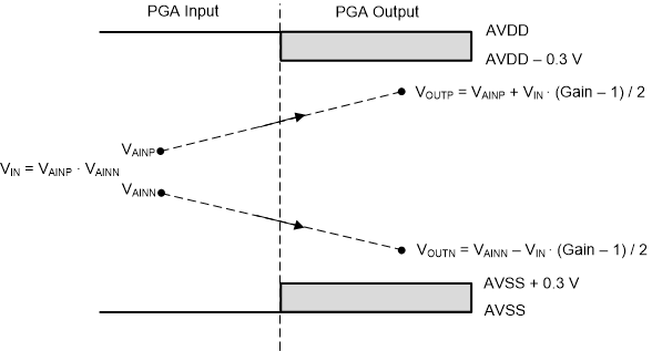
As with many amplifiers, the PGA has an input voltage range specification that must not be exceeded in order to maintain linear operation. The input range is specified as an absolute voltage (signal plus common mode voltage) at both positive and negative inputs. As specified in Equation 3, the maximum and minimum absolute input voltage depends on gain, the expected maximum differential voltage, and the minimum value of the analog power supply voltage.

Equation 3. AVSS + 0.3 V + VIN · (Gain – 1) / 2 · < VAINP and VAINN < AVDD – 0.3 V – VIN · (Gain – 1) / 2

where

  • VAINP, VAINN = absolute input voltage
  • VIN = VAINP – VAINN, maximum differential input voltage
  • Gain (for gains = 64 and 128, use 32 for calculation)
  • AVDD = minimum AVDD voltage
  • AVSS = maximum AVSS voltage

The relationship of the PGA input to the PGA output is shown graphically in Figure 41. The PGA output voltages (VOUTP, VOUTN) depend on the respective absolute input voltage, the differential input voltage, and the PGA gain. To maintain the PGA within the linear operating range, the PGA output voltages must be restricted within AVDD – 0.3 V and AVSS + 0.3 V. The diagram depicts a positive differential input voltage that results in a positive differential output voltage.
ADS1235 ai_pga_io_sbas760.gifFigure 41. PGA Input/Output Range