ZHCSHA5E july 2010 – july 2023 ADS1013-Q1 , ADS1014-Q1 , ADS1015-Q1
PRODUCTION DATA
- 1
- 1 特性
- 2 应用
- 3 说明
- 4 Revision History
- Device Comparison Table
- 5 Pin Configuration and Functions
- 6 Specifications
-
7 Detailed Description
- 7.1 Overview
- 7.2 Functional Block Diagrams
- 7.3
Feature Description
- 7.3.1 Multiplexer
- 7.3.2 Analog Inputs
- 7.3.3 Full-Scale Range (FSR) and LSB Size
- 7.3.4 Voltage Reference
- 7.3.5 Oscillator
- 7.3.6 Output Data Rate and Conversion Time
- 7.3.7 Digital Comparator (ADS1014-Q1 and ADS1015-Q1 Only)
- 7.3.8 Conversion Ready Pin (ADS1014-Q1 and ADS1015-Q1 Only)
- 7.3.9 SMbus Alert Response
- 7.4 Device Functional Modes
- 7.5 Programming
- 7.6 Register Map
-
8 Application and Implementation
- 8.1 Application Information
- 8.2
Typical Application
- 8.2.1 Design Requirements
- 8.2.2
Detailed Design Procedure
- 8.2.2.1 Shunt Resistor Considerations
- 8.2.2.2 Operational Amplifier Considerations
- 8.2.2.3 ADC Input Common-Mode Considerations
- 8.2.2.4 Resistor (R1, R2, R3, R4) Considerations
- 8.2.2.5 Noise and Input Impedance Considerations
- 8.2.2.6 First-Order RC Filter Considerations
- 8.2.2.7 Circuit Implementation
- 8.2.2.8 Results Summary
- 8.2.3 Application Curves
- 8.3 Power Supply Recommendations
- 8.4 Layout
- 9 Device and Documentation Support
- 10Mechanical, Packaging, and Orderable Information
8.2 Typical Application
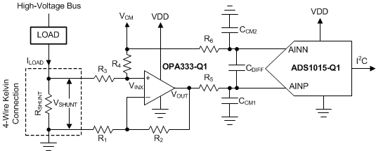
Shunt-based, current-measurement solutions are widely used to monitor load currents. Low-side, current-shunt measurements are independent of the bus voltage because the shunt common-mode voltage is near ground. Figure 8-6 shows an example circuit for a bidirectional, low-side, current-shunt measurement system. The load current is determined by measuring the voltage across the shunt resistor that is amplified and level-shifted by a low-drift operational amplifier, OPA333-Q1. The OPA333-Q1 output voltage is digitized with ADS1015-Q1 and sent to the microcontroller using the I2C interface. This circuit is capable of measuring bidirectional currents flowing through the shunt resistor with great accuracy and precision.
 Figure 8-6 Low-Side Current Shunt Monitoring