ZHCSHA5E july 2010 – july 2023 ADS1013-Q1 , ADS1014-Q1 , ADS1015-Q1
PRODUCTION DATA
- 1
- 1 特性
- 2 应用
- 3 说明
- 4 Revision History
- Device Comparison Table
- 5 Pin Configuration and Functions
- 6 Specifications
-
7 Detailed Description
- 7.1 Overview
- 7.2 Functional Block Diagrams
- 7.3
Feature Description
- 7.3.1 Multiplexer
- 7.3.2 Analog Inputs
- 7.3.3 Full-Scale Range (FSR) and LSB Size
- 7.3.4 Voltage Reference
- 7.3.5 Oscillator
- 7.3.6 Output Data Rate and Conversion Time
- 7.3.7 Digital Comparator (ADS1014-Q1 and ADS1015-Q1 Only)
- 7.3.8 Conversion Ready Pin (ADS1014-Q1 and ADS1015-Q1 Only)
- 7.3.9 SMbus Alert Response
- 7.4 Device Functional Modes
- 7.5 Programming
- 7.6 Register Map
-
8 Application and Implementation
- 8.1 Application Information
- 8.2
Typical Application
- 8.2.1 Design Requirements
- 8.2.2
Detailed Design Procedure
- 8.2.2.1 Shunt Resistor Considerations
- 8.2.2.2 Operational Amplifier Considerations
- 8.2.2.3 ADC Input Common-Mode Considerations
- 8.2.2.4 Resistor (R1, R2, R3, R4) Considerations
- 8.2.2.5 Noise and Input Impedance Considerations
- 8.2.2.6 First-Order RC Filter Considerations
- 8.2.2.7 Circuit Implementation
- 8.2.2.8 Results Summary
- 8.2.3 Application Curves
- 8.3 Power Supply Recommendations
- 8.4 Layout
- 9 Device and Documentation Support
- 10Mechanical, Packaging, and Orderable Information
8.3.2 Power-Supply Decoupling
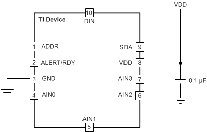
Good power-supply decoupling is important to achieve optimum performance. VDD must be decoupled with at least a 0.1-µF capacitor, as shown in Figure 8-9. The 0.1-μF bypass capacitor supplies the momentary bursts of extra current required from the supply when the device is converting. Place the bypass capacitor as close to the power-supply pin of the device as possible using low-impedance connections. Use multilayer ceramic chip capacitors (MLCCs) that offer low equivalent series resistance (ESR) and inductance (ESL) characteristics for power-supply decoupling purposes. For very sensitive systems, or for systems in harsh noise environments, avoid the use of vias for connecting the capacitors to the device pins for better noise immunity. The use of multiple vias in parallel lowers the overall inductance, and is beneficial for connections to ground planes.
 Figure 8-9 ADS1015-Q1 Power-Supply Decoupling