ZHCSEU3E July 2014 – June 2022 ADC3221 , ADC3222 , ADC3223 , ADC3224
PRODUCTION DATA
- 1 特性
- 2 应用
- 3 说明
- 4 Revision History
- 5 Pin Configuration and Functions
-
6 Specifications
- 6.1 Absolute Maximum Ratings
- 6.2 ESD Ratings
- 6.3 Recommended Operating Conditions (1)
- 6.4 Thermal Information
- 6.5 Electrical Characteristics: General
- 6.6 Electrical Characteristics: ADC3221, ADC3222
- 6.7 Electrical Characteristics: ADC3223, ADC3224
- 6.8 AC Performance: ADC3221
- 6.9 AC Performance: ADC3222
- 6.10 AC Performance: ADC3223
- 6.11 AC Performance: ADC3224
- 6.12 Digital Characteristics
- 6.13 Timing Requirements: General
- 6.14 Timing Requirements: LVDS Output
- 6.15 Typical Characteristics: ADC3221
- 6.16 Typical Characteristics: ADC3222
- 6.17 Typical Characteristics: ADC3223
- 6.18 Typical Characteristics: ADC3224
- 6.19 Typical Characteristics: Common
- 6.20 Typical Characteristics: Contour
- 7 Parameter Measurement Information
-
8 Detailed Description
- 8.1 Overview
- 8.2 Functional Block Diagram
- 8.3 Feature Description
- 8.4 Device Functional Modes
- 8.5 Programming
- 8.6
Register Maps
- 8.6.1 Summary of Special Mode Registers
- 8.6.2
Serial Register Description
- 8.6.2.1 Register 01h
- 8.6.2.2 Register 03h
- 8.6.2.3 Register 04h
- 8.6.2.4 Register 05h
- 8.6.2.5 Register 06h
- 8.6.2.6 Register 07h
- 8.6.2.7 Register 09h
- 8.6.2.8 Register 0Ah
- 8.6.2.9 Register 0Bh
- 8.6.2.10 Register 0Eh
- 8.6.2.11 Register 0Fh
- 8.6.2.12 Register 13h
- 8.6.2.13 Register 15h
- 8.6.2.14 Register 25h
- 8.6.2.15 Register 27h
- 8.6.2.16 Register 41Dh
- 8.6.2.17 Register 422h
- 8.6.2.18 Register 434h
- 8.6.2.19 Register 439h
- 8.6.2.20 Register 51Dh
- 8.6.2.21 Register 522h
- 8.6.2.22 Register 534h
- 8.6.2.23 Register 539h
- 8.6.2.24 Register 608h
- 8.6.2.25 Register 70Ah
- 9 Applications and Implementation
- 10Device and Documentation Support
- 11Mechanical, Packaging, and Orderable Information
8.3.2.1 Using the SYSREF Input
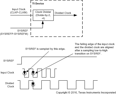
The ADC344x has a SYSREF input pin that can be used when the clock-divider feature is used. A logic low-to-high transition on the SYSREF pin aligns the falling edge of the divided clock with the next falling edge of the input clock, essentially resetting the phase of the divided clock, as shown in Figure 8-6. When multiple ADC344x devices are onboard and the clock divider option is used, the phase of the divided clock among the devices may not be the same. The phase of the divided clock in each device can be synchronized to the common sampling clock by using the SYSREF pins. SYSREF can applied as mono-shot or periodic waveform. When applied as periodic waveform, its period must be integer multiple of period of the divided clock. When not used, the SYSREFP and SYSREFM pins can be connected to AVDD and GND, respectively. Alternatively, the SYSREF buffer inside the device can be powered down using the PDN SYSREF register bit.
 Figure 8-6 Using SYSREF for Synchronization