ZHCSGI8A April 2017 – October 2021 ADC12D1620QML-SP
PRODUCTION DATA
- 1 特性
- 2 应用
- 3 说明
- 4 Revision History
- 5 Pin Configuration and Functions
-
6 Specifications
- 6.1 Absolute Maximum Ratings
- 6.2 ESD Ratings
- 6.3 Recommended Operating Conditions
- 6.4 Thermal Information
- 6.5 Converter Electrical Characteristics: Static Converter Characteristics
- 6.6 Converter Electrical Characteristics: Dynamic Converter Characteristics
- 6.7 Converter Electrical Characteristics: Analog Input/Output and Reference Characteristics
- 6.8 Converter Electrical Characteristic: Channel-to-Channel Characteristics
- 6.9 Converter Electrical Characteristics: LVDS CLK Input Characteristics
- 6.10 Electrical Characteristics: AutoSync Feature
- 6.11 Converter Electrical Characteristics: Digital Control and Output Pin Characteristics
- 6.12 Converter Electrical Characteristics: Power Supply Characteristics
- 6.13 Converter Electrical Characteristics: AC Electrical Characteristics
- 6.14 Electrical Characteristics: Delta Parameters
- 6.15 Timing Requirements: Serial Port Interface
- 6.16 Timing Requirements: Calibration
- 6.17 Quality Conformance Inspection
- 6.18 Timing Diagrams
- 6.19 Typical Characteristics
-
7 Detailed Description
- 7.1 Overview
- 7.2 Functional Block Diagram
- 7.3 Feature Description
- 7.4 Device Functional Modes
- 7.5
Programming
- 7.5.1
Control Modes
- 7.5.1.1
Non-ECM
- 7.5.1.1.1 Dual-Edge Sampling Pin (DES)
- 7.5.1.1.2 Non-Demultiplexed Mode Pin (NDM)
- 7.5.1.1.3 Dual Data-Rate Phase Pin (DDRPh)
- 7.5.1.1.4 Calibration Pin (CAL)
- 7.5.1.1.5 Low-Sampling Power-Saving Mode Pin (LSPSM)
- 7.5.1.1.6 Power-Down I-Channel Pin (PDI)
- 7.5.1.1.7 Power-Down Q-Channel Pin (PDQ)
- 7.5.1.1.8 Test-Pattern Mode Pin (TPM)
- 7.5.1.1.9 Full-Scale Input-Range Pin (FSR)
- 7.5.1.1.10 AC- or DC-Coupled Mode Pin (VCMO)
- 7.5.1.1.11 LVDS Output Common-Mode Pin (VBG)
- 7.5.1.2 Extended Control Mode
- 7.5.1.1
Non-ECM
- 7.5.1
Control Modes
- 7.6 Register Maps
- 8 Application Information Disclaimer
- 9 Power Supply Recommendations
- 10Layout
- 11Device and Documentation Support
- 12Mechanical, Packaging, and Orderable Information
6.18 Timing Diagrams
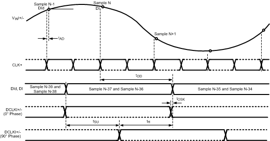 Figure 6-1 Clocking in Non-LSPSM, 1:2 Demux, Non-DES Mode*
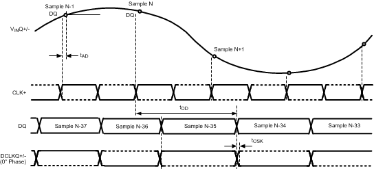 Figure 6-2 Clocking in Non-LSPSM, Non-Demux, Non-DES Mode*
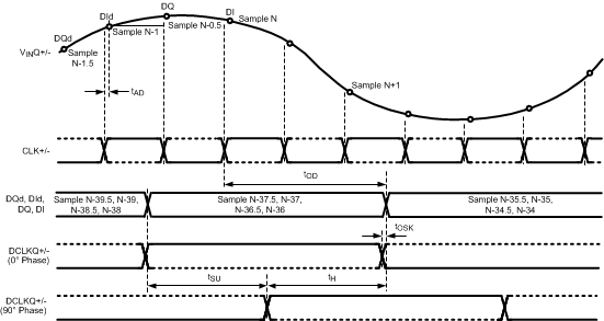 Figure 6-3 Clocking in Non-LSPSM, 1:4 Demux DES Mode*
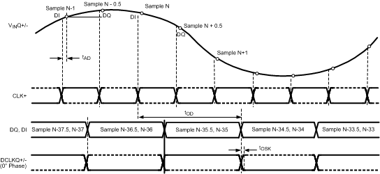 Figure 6-4 Clocking in Non-LSPSM, Non-Demux Mode DES Mode*
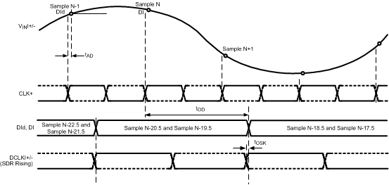 Figure 6-5 Clocking in LSPSM, 1:2 Demux Mode, Non-DES Mode*
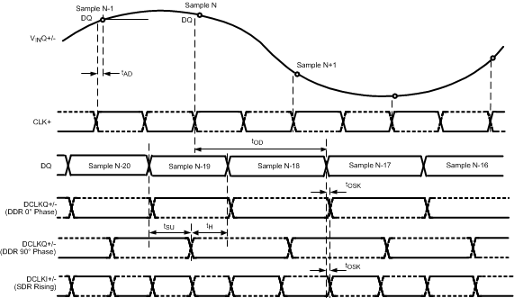 Figure 6-6 Clocking in LSPSM, Non-Demux Mode, Non-DES Mode*
* The timing for Figure 6-1 through Figure 6-6 is shown for the one input only (I or Q). However, both I and Q inputs may be used. For this case, the I channel functions precisely the same as the Q channel, with VinI, DCLKI, DId, and DI instead of VinQ, DCLKQ, DQd, and DQ. Both I and Q channel use the same CLK.
 Figure 6-7 Data Clock Reset Timing (Demux Mode)
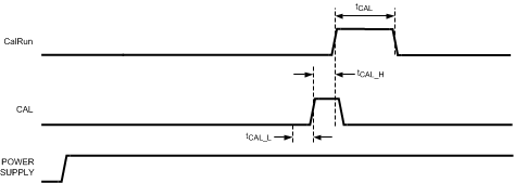 Figure 6-8 On-Command Calibration Timing
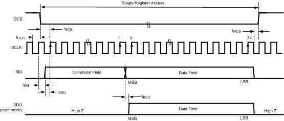 Figure 6-9 Serial Interface Timing
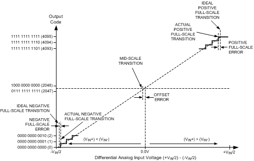 Figure 6-10 Input / Output Transfer Characteristic