SNAS308G April 2005 – May 2016 ADC081S021
PRODUCTION DATA.
- 1 Features
- 2 Applications
- 3 Description
- 4 Revision History
- 5 Device Comparison Table
- 6 Pin Configuration and Functions
- 7 Specifications
- 8 Detailed Description
- 9 Application and Implementation
- 10Power Supply Recommendations
- 11Layout
- 12Device and Documentation Support
- 13Mechanical, Packaging, and Orderable Information
9 Application and Implementation
NOTE
Information in the following applications sections is not part of the TI component specification, and TI does not warrant its accuracy or completeness. TI’s customers are responsible for determining suitability of components for their purposes. Customers should validate and test their design implementation to confirm system functionality.
9.1 Application Information
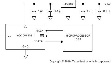
A typical application of the ADC is shown in Typical Application. Power is provided in this example by the Texas Instruments LP2950 low-dropout voltage regulator (see LP295x-N Series of Adjustable Micropower Voltage Regulators, SNVS764), available in a variety of fixed and adjustable output voltages. The power supply pin is bypassed with a capacitor network placed close to the ADC. Because the reference for the ADC is the supply voltage, any noise on the supply degrades device noise performance. To keep noise off the supply, use a dedicated linear regulator for this device, or provide sufficient decoupling from other circuitry to keep noise off the ADC supply pin. Because of the ADC's low power requirements, it is also possible to use a precision reference as a power supply to maximize performance. The three-wire interface is shown connected to a microprocessor or DSP.
9.1.1 Analog Inputs
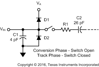
An equivalent circuit for the ADC's input is shown in Figure 23. Diodes D1 and D2 provide ESD protection for the analog inputs. At no time must the analog input go beyond (VA + 300 mV) or (GND − 300 mV), as these ESD diodes begin to conduct, which could result in erratic operation. For this reason, the ESD diodes must not be used to clamp the input signal.
The capacitor C1 in Figure 23 has a typical value of 4 pF, and is mainly the package pin capacitance. Resistor R1 is the ON resistance of the track or hold switch, and is typically 500 Ω. Capacitor C2 is the ADC sampling capacitor and is typically 26 pF. The ADC delivers best performance when driven by a low-impedance source to eliminate distortion caused by the charging of the sampling capacitance. This is especially important when using the ADC to sample AC signals. Also important when sampling dynamic signals is an anti-aliasing filter.
 Figure 23. Equivalent Input Circuit
9.1.2 Digital Inputs and Outputs
The ADC digital inputs (SCLK and CS) are not limited by the same maximum ratings as the analog inputs. The digital input pins are instead limited to 5.25 V with respect to GND, regardless of VA, the supply voltage. This allows the ADC to be interfaced with a wide range of logic levels, independent of the supply voltage.
9.2 Typical Application
The ADC081S021 is a low-power, single-channel CMOS 8-bit analog-to-digital converter that uses the supply voltage as a reference, enabling the devices to operate with a full-scale input range of 0 to VA. An example low power application with the LMT87 which is a wide range ±0.3°C (typical) accurate temperature sensor is shown in Figure 24.
 Figure 24. Typical Application Circuit
9.2.1 Design Requirements
A successful ADC081S021 and LMT87 design is contrained by the following factors:
- VIN range needs to be 0 V to VA where VA can range from 2.7 V to 5.25 V
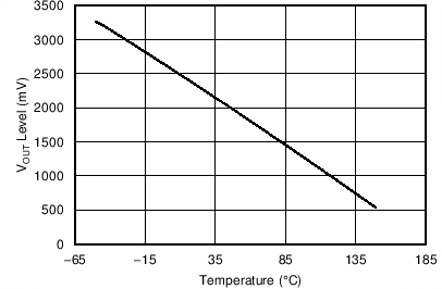
- Output level of the LMT87 can range from 538 mV to 3277 mV (which satisfies the VIN condition)
9.2.2 Detailed Design Procedure
Designing for an accurate measurement requires careful attention to timing requirements for the ADC081S021.
Because the ADC081S021 uses the supply voltage as a reference, it is important to make sure that the supply voltage is settled to its final level before exiting the shutdown mode and beginning a conversion. After the supply voltage is settled, the CS is brought to a low level (ideally 0 V) to start a conversion.
It is also important to ensure that any noise on the power supply must be less than ½ LSB in amplitude. The supply voltage must be regarded as a precise voltage reference.
After the CS is brought low, the user needs to wait for one complete conversion cycle (approximately 1 μs) for meaningful data. The dummy conversion cycle can be considered the start-up time of the ADC081S021.
The ADC081S021 digital output can then be correlated to the LMT87 output level to get an accurate temperature reading. At VDD = 2.7 V, 1 LSB of ADC081S021 is 10.54 mV. This information can be used to calculate the output level of LMT87 which can then be correlated to temperature.
9.2.3 Application Curves

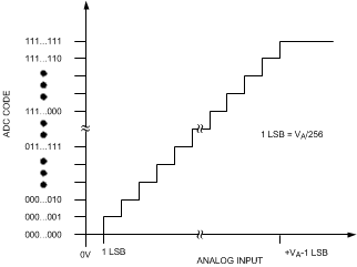
 Figure 26. Ideal Transfer Characteristic