ZHCU710 October   2019


  1.    说明
  2.    资源
  3.    特性
  4.    应用
  5.    设计图像
  6. 1System Description
    1. 1.1 Key System Specifications
  7. 2System Overview
    1. 2.1 Block Diagram
    2. 2.2 Design Considerations
    3. 2.3 Highlighted Products
      1. 2.3.1 TLV61048
      2. 2.3.2 TPS560430
      3. 2.3.3 TL431
      4. 2.3.4 CSD25310Q2
    4. 2.4 System Design Theory
      1. 2.4.1 Super Capacitor Linear Charger Circuit
      2. 2.4.2 Boost Converter Solution
      3. 2.4.3 Buck Converter Solution
  8. 3Hardware, Software, Testing Requirements, and Test Results
    1. 3.1 Required Hardware and Software
      1. 3.1.1 Hardware
    2. 3.2 Testing and Results
      1. 3.2.1 Test Setup
      2. 3.2.2 Test Results
        1. 3.2.2.1 Linear Charger Operating Waveform
        2. 3.2.2.2 Transient Waveform When Vbus fails
        3. 3.2.2.3 Super Capacitor Discharging Waveform
  9. 4Design Files
    1. 4.1 Schematics
    2. 4.2 Bill of Materials
    3. 4.3 PCB Layout Recommendations
      1. 4.3.1 Layout Prints
    4. 4.4 Altium Project
    5. 4.5 Gerber Files
    6. 4.6 Assembly Drawings
  10. 5Software Files
  11. 6Related Documentation
    1. 6.1 商标
    2. 6.2 Third-Party Products Disclaimer

Boost Converter Solution

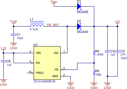
Figure 3 shows the TLV61048 boost converter, which is the main circuit of TIDA-050033. Most of the external components are selected based on the suggestion in the data sheet. The device operates at 600kHz (FREQ = floating) for higher efficiency and higher duty cycle. An external 3.3 V bias supply is applied at VIN pin so the device can operate down to 1.3 V. When Vbus exists, TLV61048 stops switching so it consumes minimum current, only 100uA (typical). Once Vbus fails, TLV61048 could work immediately and provide 12 V supply seamlessly.

Figure 3. TLV61048 Boost ConverterTIDA-050033 TLV61048BoostConverter.gif