ZHCSJW0D June   2019  – March 2020 TPS62840

PRODUCTION DATA.  

  1. 特性
  2. 应用
  3. 说明
    1.     Device Images
      1.      典型应用
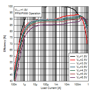
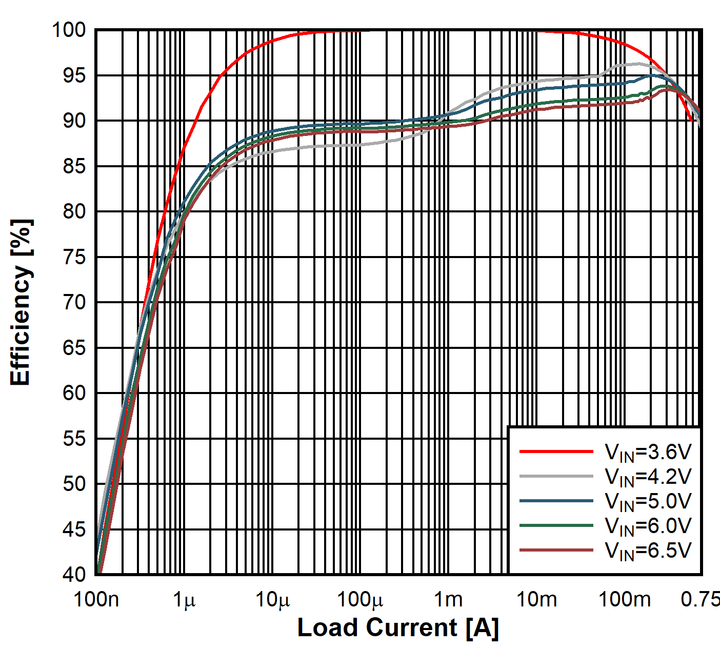
      2.      效率与负载电流间的关系 (VOUT = 1.8V)
  4. 修订历史记录
  5. Device Comparison Table
  6. Pin Configuration and Functions
    1.     Pin Functions
  7. Specifications
    1. 7.1 Absolute Maximum Ratings
    2. 7.2 ESD Ratings
    3. 7.3 Recommended Operating Conditions
    4. 7.4 Thermal Information
    5. 7.5 Electrical Characteristics
    6. 7.6 Typical Characteristics
  8. Detailed Description
    1. 8.1 Overview
    2. 8.2 Functional Block Diagram
    3. 8.3 Feature Description
      1. 8.3.1 Smart Enable and Shutdown
      2. 8.3.2 Soft Start
      3. 8.3.3 Mode Selection: Power-Save Mode (PFM/PWM) or Forced PWM Operation (FPWM)
      4. 8.3.4 Output Voltage Selection (VSET)
      5. 8.3.5 Undervoltage Lockout UVLO
      6. 8.3.6 Switch Current Limit / Short Circuit Protection
      7. 8.3.7 Output Voltage Discharge
      8. 8.3.8 Thermal Shutdown
      9. 8.3.9 STOP Mode
    4. 8.4 Device Functional Modes
      1. 8.4.1 Power-Save Mode Operation
      2. 8.4.2 Forced PWM Mode Operation
      3. 8.4.3 100% Mode Operation
  9. Application and Implementation
    1. 9.1 Application Information
    2. 9.2 Typical Application
      1. 9.2.1 Design Requirements
      2. 9.2.2 Detailed Design Procedure
        1. 9.2.2.1 Inductor Selection
        2. 9.2.2.2 Output Capacitor Selection
        3. 9.2.2.3 Input Capacitor Selection
      3. 9.2.3 Application Curves
    3. 9.3 System Example
  10. 10Power Supply Recommendations
  11. 11Layout
    1. 11.1 Layout Guidelines
    2. 11.2 Layout Example
  12. 12器件和文档支持
    1. 12.1 器件支持
      1. 12.1.1 第三方产品免责声明
    2. 12.2 保障资源
    3. 12.3 商标
    4. 12.4 静电放电警告
    5. 12.5 Glossary
  13. 13机械、封装和可订购信息

Application Curves

The conditions for the following application curves are VIN = 3.6 V, VOUT = 1.8 V, MODE = GND, STOP = GND, and the used components listed in Table 2, unless otherwise noted.
TPS62840 D1004-SLVSEC6-01.gif
RSET = GND
Figure 14. Efficiency Power Save Mode
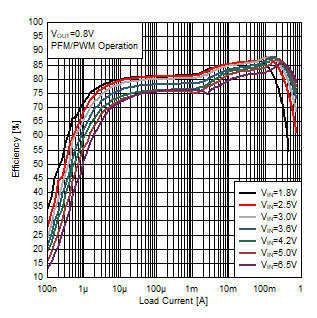
VOUT = 0.8 V
TPS62840 D1001-SLVSEC6-02.gif
RSET = GND
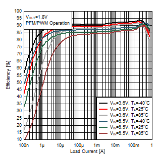
Figure 16. Efficiency Power Save Mode
VOUT = 1.8 V
TPS62840 D1006-SLVSEC6-01.gif
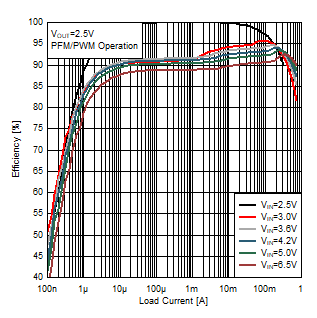
RSET = 11.5 kΩ to GND
Figure 18. Efficiency Power Save Mode
VOUT = 2.5 V
TPS62840 D003-SLVSEC6-02.gif
RSET = GND
Figure 20. Efficiency Power Save Mode
VOUT = 0.8 V for the DGR device
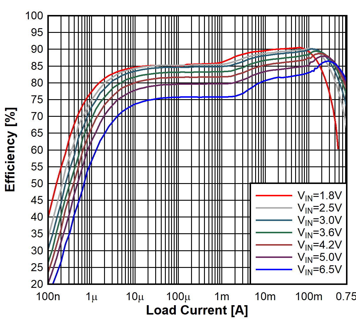
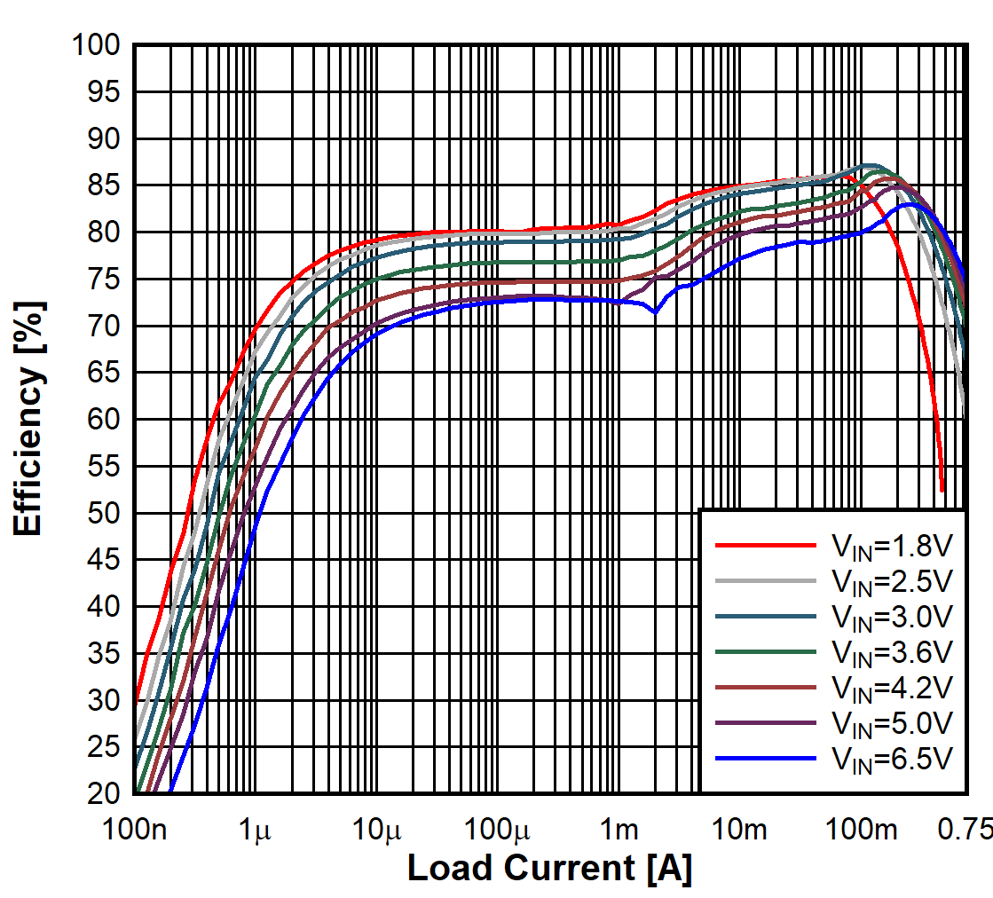
TPS62840 1.8V_Eff.gif
RSET = GND
Figure 22. Efficiency Power Save Mode
VOUT = 1.8 V for the DGR device
TPS62840 D1007-SLVSEC6-01.gif
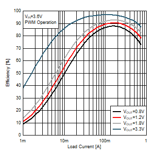
Figure 24. Efficiency Forced PWM Mode
VOUT = 0.8 V / 1.2 V / 1.8 V / 3.3 V
TPS62840 D3001-SLVSEC6-01.gif
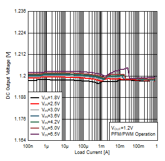
RSET = 15.8k Ω to GND
Figure 26. Output Voltage versus Load Current
VOUT = 1.2 V
TPS62840 D3003-SLVSEC6-01.gif
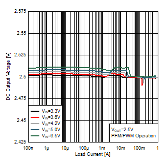
RSET = 11.5 kΩ to GND
Figure 28. Output Voltage versus Load Current
VOUT = 2.5 V
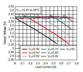
TPS62840 D3300-SLVSEC6-01.gif
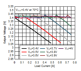
RSET = GND
Figure 30. Output Voltage versus Load Current
VOUT = 3.4 V
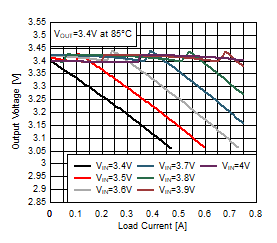
TPS62840 D3302-SLVSEC6-01.gif
RSET = GND
Figure 32. Output Voltage versus Load Current
VOUT = 3.4 V
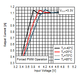
TPS62840 D3400-SLVSEC6-01.gif
RSET = 267 kΩ to GND
Figure 34. Maximum Output Current versus Input Voltage
VOUT = 3.3 V
TPS62840 D3101-SLVSEC6-01.gif
RSET = 15.8 kΩ to GND
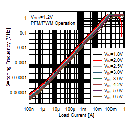
Figure 36. Switching Frequency versus Load Current
VOUT = 1.2 V
TPS62840 D3103-SLVSEC6-01.gif
RSET = 267 kΩ to GND
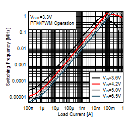
Figure 38. Switching Frequency versus Load Current
VOUT = 3.3 V
TPS62840 D3106-SLVSEC6-01.gif
RSET = 267 kΩ to GND
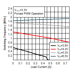
Figure 40. Switching Frequency versus Load Current
VOUT = 3.3 V
TPS62840 D3201-SLVSEC6-01.gif
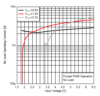
Figure 42. No Load Operating Current versus Input Voltage
TPS62840 D003-SLVSEC6-01.gif
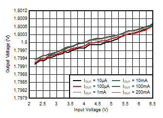
EN = VIN MODE = HIGH
Figure 44. Output Voltage Accuracy (Line Regulation)
TPS62840 PWMOp_1Vout8_3Vin6_10mA(7)_2.png
VOUT = 1.8 V
MODE = HIGH
IOUT = 10 mA
Figure 46. Output Voltage Ripple, PWM Operation
TPS62840 LineTransient_1V8_500mA_2.png
VOUT = 1.8 V
rise/fall time = 20 µs
VIN = 2.5 V to 6.5 V
IOUT = 500 mA
Figure 48. Line Transient PWM Mode
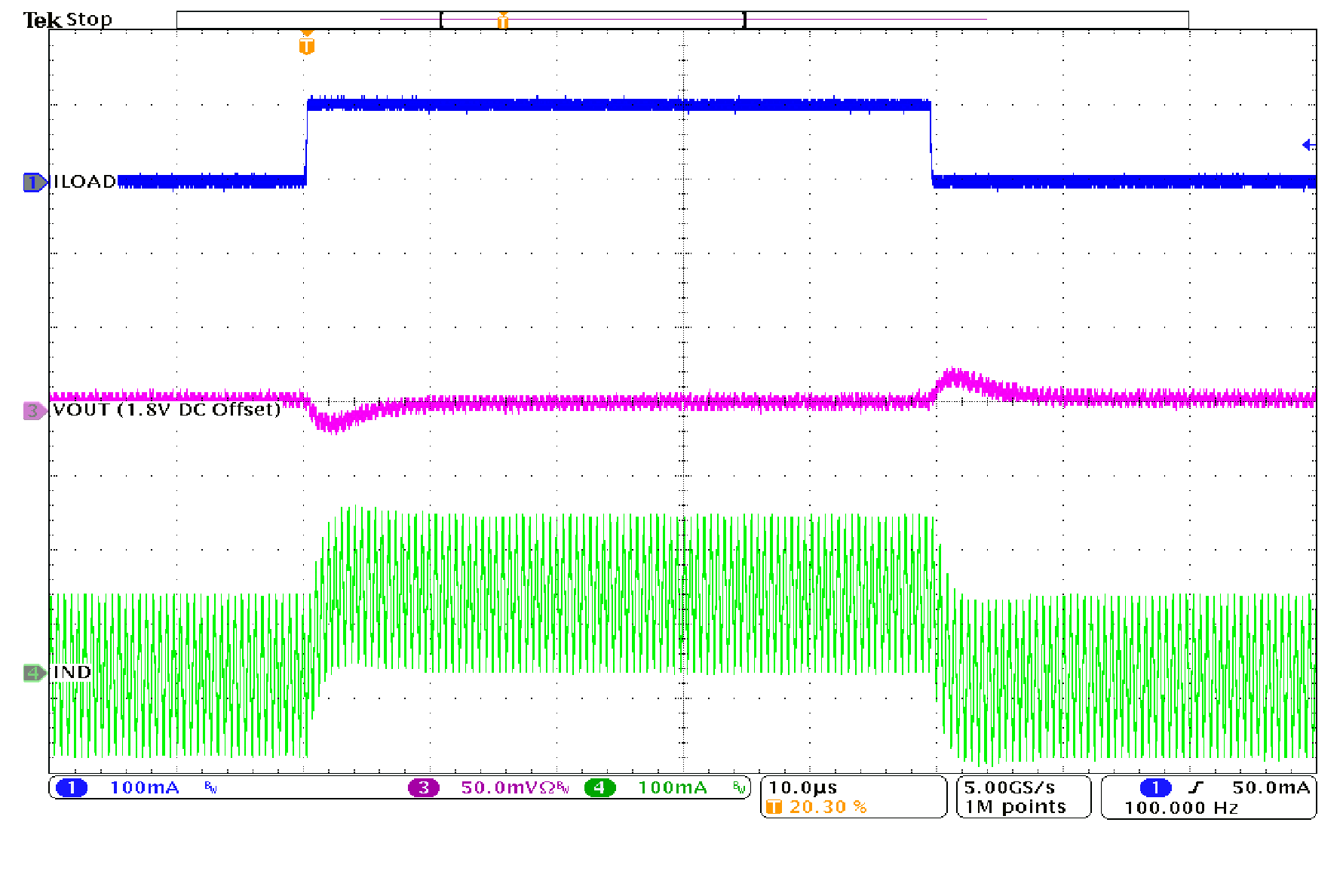
TPS62840 LoadTransient_1V8_125mAto375mA_2.png
VOUT = 1.8 V
rise/fall time < 1 µs
VIN = 3.6 V
IOUT = 125 mA to 375 mA
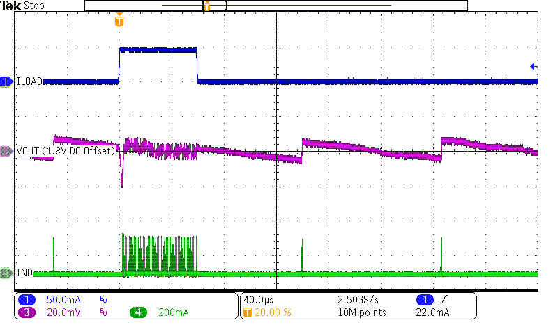
Figure 50. Load Transient PFM/PWM Mode
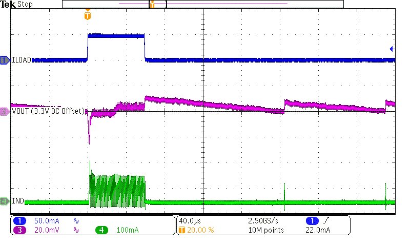
TPS62840 LoadTransient_3V3_75uAto50mA_2.png
VOUT = 3.3 V
rise/fall time < 1 µs
VIN = 3.6 V
IOUT = 75 µA to 50 mA
Figure 52. Load Transient PFM Mode
TPS62840 TurnOnOff_viaEN_1Vout8_0mA_3Vin6(0)_2.png
VOUT = 1.8 V
Turned on by EN input
VIN = 3.6 V
IOUT = 0 mA
Figure 54. Start-up/Shutdown into No Load
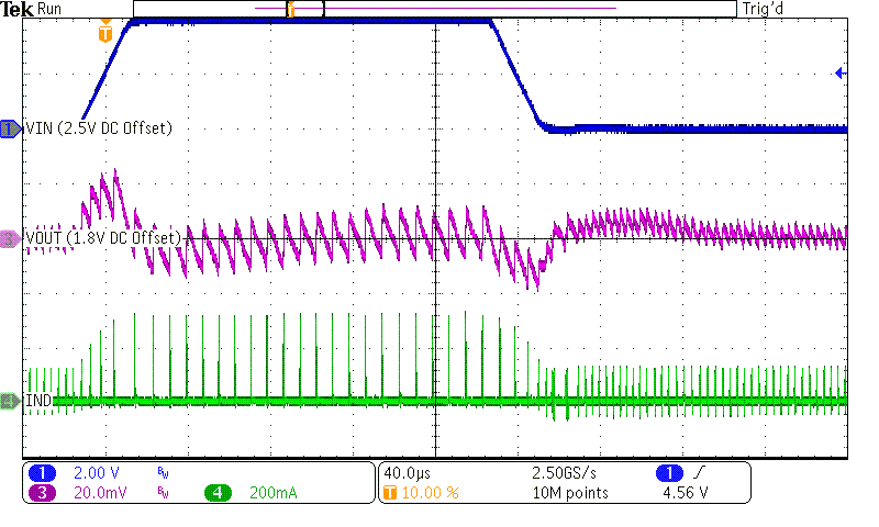
TPS62840 TurnOnOff_viaUVLO_1Vout8_0mA_3Vin6(3)_2.png
VOUT = 1.8 V
VIN rising from 0 V to 3.6 V
EN = VIN
IOUT = 0 mA
Figure 56. Start-up/Shutdown into No Load
TPS62840 STOP_1Vout8_10mA_3Vin6_PFM(5)_2.png
VOUT = 1.8 V
PFM Operation
VIN = 3.6 V
IOUT = 10 mA
Figure 58. STOP Mode Operation
TPS62840 D1005-SLVSEC6-01.gif
RSET = 15.8 kΩ to GND
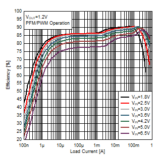
Figure 15. Efficiency Power Save Mode
VOUT = 1.2 V
TPS62840 D1002-SLVSEC6-01.gif
RSET = GND
Figure 17. Efficiency Power Save Mode
VOUT = 1.8 V
TPS62840 D1003-SLVSEC6-01.gif
RSET = 267 kΩ to GND
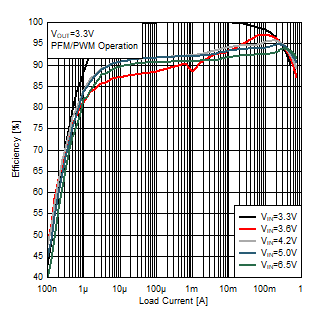
Figure 19. Efficiency Power Save Mode
VOUT = 3.3 V
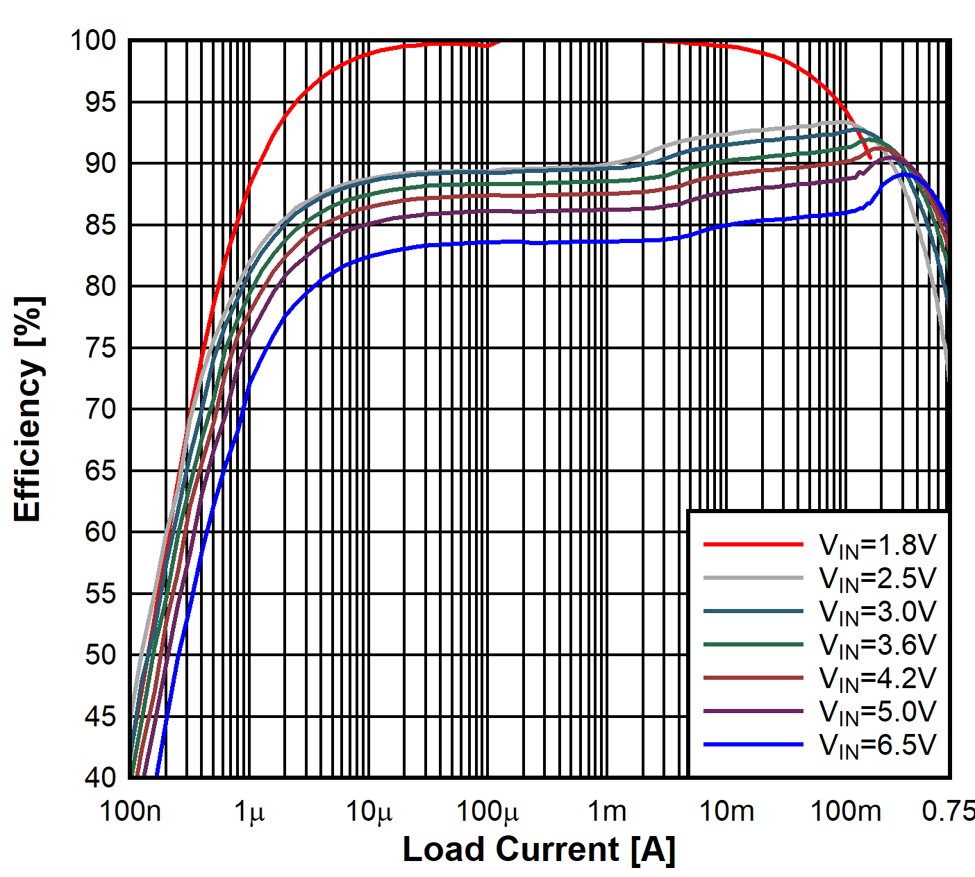
TPS62840 D003-SLVSEC6-04.gif
RSET = GND
Figure 21. Efficiency Power Save Mode
VOUT = 1.2 V for the DGR device
TPS62840 3.6V_Eff.gif
RSET = 267 kΩ to GND
Figure 23. Efficiency Power Save Mode
VOUT = 3.6 V for the DGR device
TPS62840 D3000-SLVSEC6-01.gif
RSET = GND
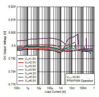
Figure 25. Output Voltage versus Load Current
VOUT = 0.8 V
TPS62840 D3002-SLVSEC6-01.gif
RSET = GND
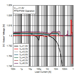
Figure 27. Output Voltage versus Load Current
VOUT = 1.8 V
TPS62840 D3004-SLVSEC6-01.gif
RSET = 267 kΩ to GND
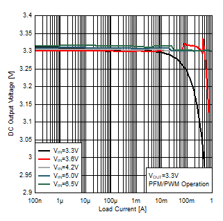
Figure 29. Output Voltage versus Load Current
VOUT = 3.3 V
TPS62840 D3301-SLVSEC6-01.gif
RSET = GND
Figure 31. Output Voltage versus Load Current
VOUT = 3.4 V
TPS62840 D3401-SLVSEC6-01.gif
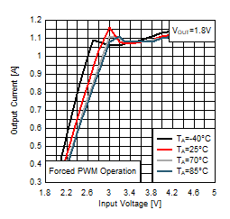
RSET = GND
Figure 33. Maximum Output Current versus Input Voltage
VOUT = 1.8 V
TPS62840 D3100-SLVSEC6-01.gif
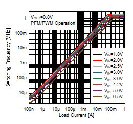
RSET = GND
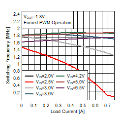
Figure 35. Switching Frequency versus Load Current
VOUT = 0.8 V
TPS62840 D3102-SLVSEC6-01.gif
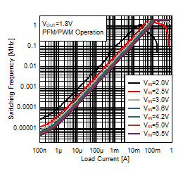
RSET = GND
Figure 37. Switching Frequency versus Load Current
VOUT = 1.8 V
TPS62840 D3105-SLVSEC6-01.gif
RSET = GND
Figure 39. Switching Frequency versus Load Current
VOUT = 1.8 V
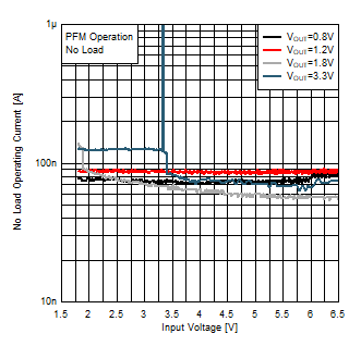
TPS62840 D3200-SLVSEC6-01.gif
Figure 41. No Load Operating Current versus Input Voltage
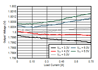
TPS62840 D002-SLVSEC6-01.gif
EN = VIN MODE = HIGH
Figure 43. Output Voltage Accuracy (Load Regulation)
TPS62840 PFMOp_1Vout8_3Vin6_10mA(6)_2.png
VOUT = 1.8 V IOUT = 10 mA
Figure 45. Output Voltage Ripple, PFM Operation
TPS62840 LineTransient_1V8_1mA_2.png
VOUT = 1.8 V
rise/fall time = 20 µs
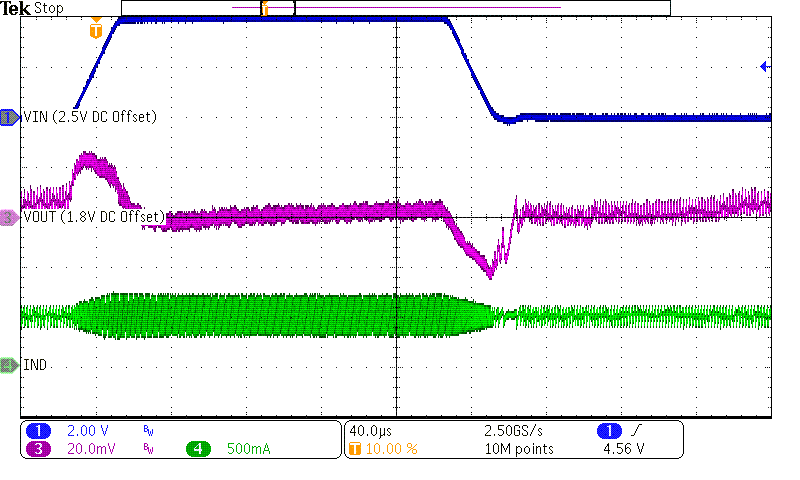
VIN = 2.5 V to 6.5 V
IOUT = 10 mA
Figure 47. Line Transient PFM Mode
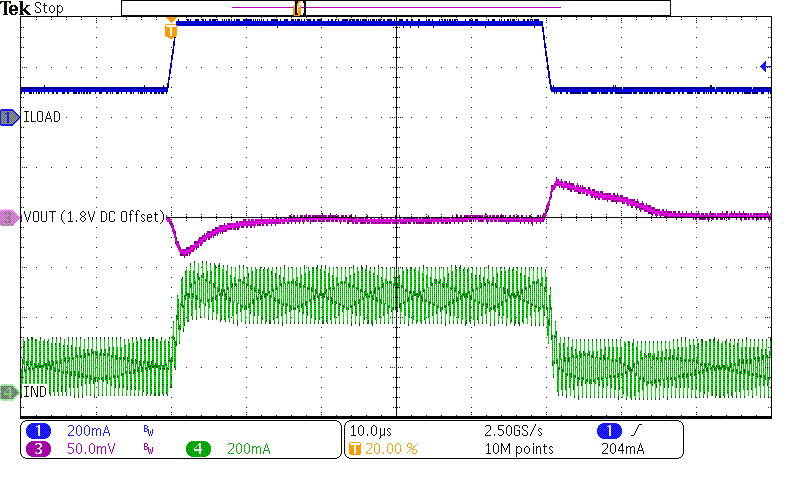
TPS62840 LoadTransient_1V8_125uAto50mA_2.png
VOUT = 1.8 V
rise/fall time < 1 µs
VIN = 3.6 V
IOUT = 125 µA to 50 mA
Figure 49. Load Transient PFM Mode
TPS62840 TPS62842_Load_Transient_0mA_100mA.png
VOUT = 1.8 V
rise/fall time < 1 µs
VIN = 3.6 V
IOUT = 0 A to 100 mA
Figure 51. Load Transient PWM Mode from No load
TPS62840 100Mode_3Vou3_50mA(4)_2.png
VOUT = 3.3 V VIN = 3.1 V to 3.6 V
IOUT = 50 mA
Figure 53. 100% Mode Entry/Exit Operation
TPS62840 TurnOnOff_viaEN_1Vout8_4R5_3Vin6(1)_2.png
VOUT = 1.8 V
Turned on by EN input
VIN = 3.6 V
IOUT = 400 mA
RLOAD = 4.5 Ω
Figure 55. Start-up/Shutdown into Load
TPS62840 TurnOnOff_viaEN_3Vout3_0mA_3Vin6(2)_2.png
VOUT = 3.3 V
Turned on by EN input
VIN = 3.6 V
IOUT = 0 mA
Figure 57. Start-up/Shutdown into No Load
TPS62840 STOP_1Vout8_10mA_3Vin6_FPWM(8)_2.png
VOUT = 1.8 V
PWM Operation
VIN = 3.6 V
IOUT = 10 mA
Figure 59. STOP Mode Operation