• Menu
  • Product
  • Email
  • PDF
  • Order now
  • LM7600x-Q1 3.5V 至 60V、2.5A/3.5A 同步降压稳压器

    • ZHCSH62B December   2017  – October 2019 LM76002-Q1 , LM76003-Q1

      PRODUCTION DATA.  

  • CONTENTS
  • SEARCH
  • LM7600x-Q1 3.5V 至 60V、2.5A/3.5A 同步降压稳压器
  1. 1 特性
  2. 2 应用
  3. 3 说明
    1.     简化原理图
    2.     效率与输出电流(VOUT = 5V,fSW = 400kHz,自动模式)
  4. 4 修订历史记录
  5. 5 Pin Configuration and Functions
    1.     Pin Functions
  6. 6 Specifications
    1. 6.1 Absolute Maximum Ratings
    2. 6.2 ESD Ratings
    3. 6.3 Recommended Operating Conditions
    4. 6.4 Thermal Information
    5. 6.5 Electrical Characteristics
    6. 6.6 Timing Characteristics
    7. 6.7 Switching Characteristics
    8. 6.8 System Characteristics
    9. 6.9 Typical Characteristics
  7. 7 Detailed Description
    1. 7.1 Overview
    2. 7.2 Functional Block Diagram
    3. 7.3 Feature Description
      1. 7.3.1  Fixed-Frequency, Peak-Current-Mode Control
      2. 7.3.2  Light Load Operation Modes — PFM and FPWM
      3. 7.3.3  Adjustable Output Voltage
      4. 7.3.4  Enable (EN Pin) and UVLO
      5. 7.3.5  Internal LDO, VCC UVLO, and Bias Input
      6. 7.3.6  Soft Start and Voltage Tracking (SS/TRK)
      7. 7.3.7  Adjustable Switching Frequency (RT) and Frequency Synchronization
      8. 7.3.8  Minimum On-Time, Minimum Off-Time, and Frequency Foldback at Dropout Conditions
      9. 7.3.9  Internal Compensation and CFF
      10. 7.3.10 Bootstrap Voltage and VBOOT UVLO (BOOT Pin)
      11. 7.3.11 Power Good and Overvoltage Protection (PGOOD)
      12. 7.3.12 Overcurrent and Short-Circuit Protection
      13. 7.3.13 Thermal Shutdown
    4. 7.4 Device Functional Modes
      1. 7.4.1 Shutdown Mode
      2. 7.4.2 Standby Mode
      3. 7.4.3 Active Mode
      4. 7.4.4 CCM Mode
      5. 7.4.5 DCM Mode
      6. 7.4.6 Light Load Mode
      7. 7.4.7 Foldback Mode
      8. 7.4.8 Forced Pulse-Width-Modulation Mode
      9. 7.4.9 Self-Bias Mode
  8. 8 Application and Implementation
    1. 8.1 Application Information
    2. 8.2 Typical Applications
      1. 8.2.1 Design Requirements
      2. 8.2.2 Detailed Design Procedure
        1. 8.2.2.1  Custom Design With WEBENCH® Tools
        2. 8.2.2.2  Output Voltage Setpoint
        3. 8.2.2.3  Switching Frequency
        4. 8.2.2.4  Input Capacitors
        5. 8.2.2.5  Inductor Selection
        6. 8.2.2.6  Output Capacitor Selection
        7. 8.2.2.7  Feed-Forward Capacitor
        8. 8.2.2.8  Bootstrap Capacitors
        9. 8.2.2.9  VCC Capacitors
        10. 8.2.2.10 BIAS Capacitors
        11. 8.2.2.11 Soft-Start Capacitors
        12. 8.2.2.12 Undervoltage Lockout Setpoint
        13. 8.2.2.13 PGOOD
        14. 8.2.2.14 Synchronization
      3. 8.2.3 Application Curves
  9. 9 Power Supply Recommendations
  10. 10Layout
    1. 10.1 Layout Guidelines
      1. 10.1.1 Layout Highlights
      2. 10.1.2 Compact Layout for EMI Reduction
      3. 10.1.3 Ground Plane and Thermal Considerations
      4. 10.1.4 Feedback Resistors
    2. 10.2 Layout Example
    3. 10.3 Thermal Design
  11. 11器件和文档支持
    1. 11.1 器件支持
      1. 11.1.1 开发支持
        1. 11.1.1.1 使用 WEBENCH® 工具创建定制设计
    2. 11.2 接收文档更新通知
    3. 11.3 支持资源
    4. 11.4 商标
    5. 11.5 静电放电警告
    6. 11.6 Glossary
  12. 12机械、封装和可订购信息
  13. 重要声明
search No matches found.
  • Full reading width
    • Full reading width
    • Comfortable reading width
    • Expanded reading width
  • Card for each section
  • Card with all content


DATA SHEET

LM7600x-Q1 3.5V 至 60V、2.5A/3.5A 同步降压稳压器

本资源的原文使用英文撰写。 为方便起见,TI 提供了译文;由于翻译过程中可能使用了自动化工具,TI 不保证译文的准确性。 为确认准确性,请务必访问 ti.com 参考最新的英文版本(控制文档)。

1 特性

  • 具有符合面向汽车应用的 AEC-Q100 标准
    • 器件温度 1 级:-40℃ 至 +125℃ 的环境运行温度范围
    • 器件 HBM ESD 分类等级 2
    • 器件 CDM ESD 分类等级 C5
  • 集成同步整流
  • 输入电压 3.5V 至 60V(最大值 65V)
  • 输出电压 1V 至 95% VIN
  • 稳压静态电流 15µA
  • 宽电压转换范围
    • tON-MIN = 65ns(典型值)
    • tOFF-MIN = 95ns(典型值)
  • 系统级 特性
    • 与外部时钟保持同步
    • 电源正常状态标志
    • 可调软启动(默认为 6.3ms)
  • 引脚可选式 FPWM 运行
  • 可调频率范围:300kHz 至 2.2MHz
  • 在轻负载架构下实现高效率 (PFM)
  • 保护 功能
    • 逐周期电流限制
    • 具有断续模式的短路保护
    • 过热关断保护
  • 使用 LM76002-Q1η/LM76003-Q1 并借助 WEBENCH® 电源设计器创建定制设计方案

2 应用

  • 商用车辆 摄像头 应用
  • 信息娱乐系统和仪表组
  • 混合动力电动汽车
  • 电动汽车

3 说明

LM76002-Q1/LM76003-Q1 稳压器是一款易于使用的同步降压直流/直流转换器,能驱动高达 2.5A (LM76002-Q1) 或 3.5A (LM76003-Q1) 的负载电流,输入电压最高可达 60V。LM76002-Q1/LM76003-Q1 解决方案尺寸极小,但能提供优异的效率和输出精度。采用峰值电流模式控制。可调 特性 (例如可调开关频率、同步、FPWM 选项、电源正常状态标志、精密使能端、可调式软启动和跟踪)可为各种应用提供灵活且简单易用的 解决方案。轻负载时的自动频率折返和可选的外部偏置电源可以提高效率。该器件需要极少的外部组件,其引脚专为简化 PCB 布局而设计,可提供优异的 EMI (CISPR25) 和热性能。保护 功能 包括输入欠压锁定、热关断、逐周期电流限制和短路保护。LM76002-Q1/LM76003-Q1 器件采用 WQFN 30 引脚无引线式封装,且具有可湿性侧面。

器件信息(1)

器件型号 封装 封装尺寸(标称值)
LM76002-Q1 WQFN (30) 6.00mm × 4.00mm
LM76003-Q1
  1. 如需了解所有可用封装,请参阅数据表末尾的可订购产品附录。

空白

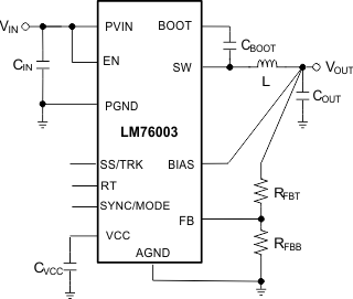
简化原理图

LM76002-Q1 LM76003-Q1 SimplifiedSchFP-.gif

效率与输出电流
(VOUT = 5V,fSW = 400kHz,自动模式)
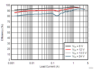
LM76002-Q1 LM76003-Q1 D034-tc-eff-auto-5vout-400k-snvsau3.gif

4 修订历史记录

Changes from A Revision (November 2018) to B Revision

  • Updated the Thermal Information table.Go
  • Changed Figure 17Go
  • Updated Power Good and Overvoltage Protection (PGOOD) sectionGo

5 Pin Configuration and Functions

RNP Package
30-Pin WQFN
Top View
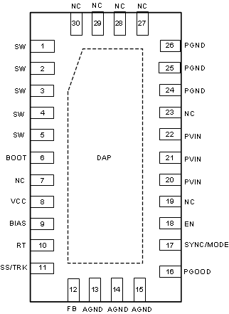
LM76002-Q1 LM76003-Q1 Pin_Out.gif

Pin Functions

PIN I/O(1) DESCRIPTION
NO. NAME
1, 2, 3, 4, 5 SW P Switching output of the regulator. Internally connected to source of the HS FET and drain of the LS FET. Connect to power inductor and boot-strap capacitor.
6 BOOT P Boot-strap capacitor connection for high-side driver. Connect a high-quality 470-nF capacitor from this pin to the SW pin.
7, 19, 23, 27, 28, 29, 30 NC — Not internally connected. Connect to ground copper on PCB to improve heat-sinking of the device and board level reliability.
8 VCC P Output of internal bias supply. Used as supply to internal control circuits. Connect a high-quality 2.2-µF capacitor from this pin to GND. TI does not recommended loading this pin by external circuitry.
9 BIAS P Optional BIAS LDO supply input. TI recommends tying this to VOUT when 3.3 V ≤ VOUT ≤ 18 V, or tying to an external 3.3-V or 5-V rail if available, to improve efficiency. When used, place a 1-µF capacitor from this terminal to ground. Tie to ground when not in use.
10 RT A Switching frequency setting pin. Place a resistor from this pin to ground to set the switching frequency. If floating, the default switching frequency is 500 kHz. Do not short to ground.
11 SS/TRK A Soft-start-control pin. Leave this pin floating to use the 6.3-ms internal soft-start ramp. An external capacitor can be connected from this pin to ground to extend the soft-start time. A 2-µA current sourced from this pin can charge the capacitor to provide the ramp. Connect to external ramp for tracking. Do not short to ground.
12 FB A Feedback input for output voltage regulation. Connect a resistor divider to set the output voltage. Never short this terminal to ground during operation.
16 PGOOD A Open-drain power-good flag output. Connect to suitable voltage supply through a current limiting resistor. High = VOUT regulation OK, Low = VOUT regulation fault. PGOOD = Low when EN = Low.
17 SYNC/MODE A Synchronization input and mode setting pin. Do not float, tie to ground if not used. Tie to ground: DCM/PFM operation under light loads, improved efficiency; tie to logic high: forced PWM under light loads, constant switching frequency over load; tie to external clock source: synchronize switching action to the clock, forced PWM under light loads. Triggers on the rising edge of external clock.
18 EN A Precision-enable input to regulator. Do not float. High = on, Low = off. Can be tied to VIN. Precision-enable input allows adjustable UVLO by external resistor divider.
13, 14, 15 AGND G Analog ground. Ground reference for internal references and logic. All electrical parameters are measured with respect to this pin. Connect to system ground on PCB.
20, 21, 22 PVIN P Supply input to internal bias LDO and HS FET. Connect to input supply and input bypass capacitors CIN. CIN must be placed right next to this pin and PGND and connected with short traces.
24, 25, 26 PGND G Power ground, connected to the source of LS FET internally. Connect to system ground, DAP/EP, AGND, ground side of CIN and COUT. Path to CIN must be as short as possible.
EP DAP — Low impedance connection to AGND. Connect to system ground on PCB. Major heat dissipation path for the die. Must be used for heat sinking by soldering to ground copper on PCB. Thermal vias are preferred.
(1) A = Analog, O = Output, I = Input, G = Ground, P = Power

6 Specifications

6.1 Absolute Maximum Ratings

over operating free-air temperature range of –40°C to +125°C (unless otherwise noted)(1)
PARAMETER MIN MAX UNIT
Input voltages PVIN to PGND –0.3 65 V
EN to AGND –0.3 VIN + 0.3
FB, RT, SS/TRK to AGND –0.3 5
PGOOD to AGND –0.1 20
SYNC to AGND –0.3 5.5
BIAS to AGND –0.3 Lower of (VIN + 0.3) or 30
AGND to PGND –0.3 0.3
Output voltages SW to PGND –0.3 VIN + 0.3 V
SW to PGND less than 10-ns transients –3.5 65
BOOT to SW –0.3 5.5
VCC to AGND –0.3 5.5
Junction temperature, TJ –40 150 °C
Storage temperature, Tstg –65 150 °C
(1) Stresses beyond those listed under Absolute Maximum Ratings may cause permanent damage to the device. These are stress ratings only, which do not imply functional operation of the device at these or anyother conditions beyond those indicated under Recommended OperatingConditions. Exposure to absolute-maximum-rated conditions for extended periods may affect device reliability.

6.2 ESD Ratings

VALUE UNIT
V(ESD) Electrostatic discharge Human-body model (HBM), per AEC Q100-002(1) ±2000 V
Charged-device model (CDM), per AEC Q100-011 ±750 V
(1) AEC Q100-002 indicates that HBM stressing shall be in accordance with the ANSI/ESDA/JEDEC JS-001 specification.

6.3 Recommended Operating Conditions

over operating free-air temperature range (unless otherwise noted)(1)
MIN MAX UNIT
Input voltages PVIN to PGND 3.5 60 V
EN 0 VIN
FB 0 4.5
PGOOD 0 18
BIAS input not used 0 0.3
BIAS input used 0 Lower of (VIN + 0.3) or 24
AGND to PGND –0.1 0.1
Output voltage VOUT 1 95% of VIN V
Output current IOUT, LM76002-Q1 0 2.5 A
IOUT, LM76003-Q1  0 3.5
(1) Recommended operating rating indicate conditions for which the device is intended to be functional, but do not ensure specific performance limits. For ensured specifications, see Electrical Characteristics.

6.4 Thermal Information

THERMAL METRIC(1) LM76002/LM76003 UNIT
RNP (WQFN)
30 PINS
RθJA Junction-to-ambient thermal resistance 29.6 °C/W
RθJC(top) Junction-to-case (top) thermal resistance 17.6 °C/W
RθJB Junction-to-board thermal resistance 9.1 °C/W
ψJT Junction-to-top characterization parameter 0.2 °C/W
ψJB Junction-to-board characterization parameter 9.0 °C/W
RθJC(bot) Junction-to-case (bottom) thermal resistance 1.0 °C/W
(1) For more information about traditional and new thermal metrics, see the Semiconductor and IC Package Thermal Metrics application report.

6.5 Electrical Characteristics

Limits apply over the recommended operating junction temperature (TJ) range of –40°C to +125°C, unless otherwise stated. Minimum and maximum limits are specified through test, design, or statistical correlation. Typical values represent the most likely parametric norm at TJ = 25°C, and are provided for reference purposes only. Unless otherwise stated, the following conditions apply: VIN= 24 V.
PARAMETER TEST CONDITIONS MIN TYP MAX UNIT
SUPPLY VOLTAGE (PVIN PINS)
VIN Operating input voltage range 3.5 60 V
ISD Shutdown quiescent current; measured at PVIN pin(1) VEN = 0 V
TJ = 25℃
1.2 10 µA
IQ_NONSW Operating quiescent current from VIN (non-switching) VEN = 2 V, VFB = 1.5 V, VBIAS = 3.3 V external 0.9 12 µA
ENABLE (EN PIN)
VEN_VCC_H Enable input high level for VCC output VEN rising 1.2 V
VEN_VCC_L Enable input low level for VCC output VEN falling 0.3 V
VEN_VOUT_H Enable input high level for VOUT VEN rising 1.14 1.204 1.25 V
VEN_VOUT_HYS Enable input hysteresis for VOUT VEN falling hysteresis –150 mV
ILKG_EN Enable input leakage current VEN = 2 V 1.4 200 nA
INTERNAL LDO (VCC PIN, BIAS PIN)
VCC Internal VCC voltage PWM operation 3.29 V
PFM operation 3.1 V
VCC_UVLO Internal VCC undervoltage lockout VCC rising 2.96 3.14 3.27 V
VCC falling hysteresis –565 mV
VBIAS_ON Input changeover VBIAS rising 3.11 3.25 V
VBIAS falling hysteresis –63 mV
IBIAS_NONSW Operating quiescent current from external VBIAS (non-switching) VEN = 2 V, VFB = 1.5 V, VBIAS = 3.3 V external 21 50 µA
VOLTAGE REFERENCE (FB PIN)
VFB Feedback voltage PWM mode 0.987 1.006 1.017 V
ILKG_FB Input leakage current at FB pin VFB = 1 V 0.2 60 nA
HIGH SIDE DRIVER (BOOT PIN)
VBOOT_UVLO BOOT - SW undervoltage lockout 1.6 2.2 2.7 V
CURRENT LIMITS AND HICCUP
IHS_LIMIT​​​​​​(2) Short-circuit, high-side current limit LM76002-Q1 3.2 4.2 5.3 A
LM76003-Q1 4.35 5.5 6.8
ILS_LIMIT(2) Low-side current limit LM76002-Q1 2.3 3.2 4.2 A
LM76003-Q1 3.4 4.2 5.3
INEG_LIMIT Negative current limit LM76002-Q1 –2.5 A
LM76003-Q1 –3.3
VHICCUP Hiccup threshold on FB pin 0.38 0.42 0.46 V
IL_ZC Zero cross-current limit 0.05 A
SOFT START (SS/TRK PIN)
ISSC Soft-start charge current 1.8 2 2.2 µA
RSSD Soft-start discharge resistance UVLO, TSD, OCP; or EN = 0 V 2 kΩ
POWER GOOD (PGOOD PIN) and OVERVOLTAGE PROTECTION
VPGOOD_OV Power-good overvoltage threshold % of FB voltage 106% 110% 113%
VPGOOD_UV Power-good undervoltage threshold % of FB voltage 86% 90% 93%
VPGOOD_HYS Power-good hysteresis % of FB voltage 2.5%
VPGOOD_VALID Minimum input voltage for proper PGOOD function 50-µA pullup to PGOOD pin, VEN = 0 V, TJ = 25°C 1.3 2 V
RPGOOD Power-good on-resistance VEN = 2.5 V 40 100 Ω
VEN = 0 V 30 90
MOSFETS
RDS_ON_HS(3) High-side MOSFET on-resistance IOUT  = 1 A, VBIAS = VOUT = 3.3 V 95 150 mΩ
RDS_ON_LS(3) Low-side MOSFET on-resistance IOUT  = 1 A, VBIAS = VOUT = 3.3 V 45 85 mΩ
THERMAL SHUTDOWN
TSD(4) Thermal shutdown threshold Shutdown threshold 160 °C
Recovery threshold 135
(1) Shutdown current includes leakage current ofthe switching transistors.
(2) This current limit was measured as the internal comparator trip point. Due to inherent delays in the current limit comparator and drivers, the peak current limit measured in closed loop with faster slew rate will be larger, and valley current limit will be lower.
(3) Measured at pins.
(4) Ensured by design.

6.6 Timing Characteristics

MIN NOM MAX UNIT
CURRENT LIMITS AND HICCUP
NOC(1) Number of switching cycles before hiccup is tripped 128 Cycles
tOC Overcurrent hiccup retry delay time 46 ms
SOFT START (SS/TRK PIN)
tSS Internal soft-start time CSS = OPEN, from EN rising edge to PGOOD rising edge 3.5 6.3 ms
POWER GOOD (PGOOD PIN) and OVERVOLTAGE PROTECTION
tPGOOD_RISE PGOOD rising edge deglitch delay 80 140 200 µs
tPGOOD_FALL PGOOD falling edge deglitch delay 80 140 200 µs
(1) Ensured by design.

6.7 Switching Characteristics

PARAMETER TEST CONDITIONS MIN TYP MAX UNIT
PWM LIMITS (SW PINS)
tON-MIN Minimum switch on-time 65 95 ns
tOFF-MIN Minimum switch off-time 95 130 ns
tON-MAX Maximum switch on-time HS timeout in dropout 3.8 8 11.4 µs
OSCILLATOR (RT and SYNC PINS)
fOSC Internal oscillator frequency RT = Open 440 500 560 kHz
fADJ Minimum adjustable frequency by RT or SYNC RT =133 kΩ, 0.1% 270 300 330 kHz
Maximum adjustable frequency by RT or SYNC RT = 17.4 kΩ, 0.1% 1980 2200 2420
VSYNC_HIGH Sync input high level threshold 2 V
VSYNC_LOW Sync input low level threshold 0.4 V
VMODE_HIGH Mode input high level threshold for FPWM 0.42 V
VMODE_LOW Mode input low level threshold for AUTO mode 0.4 V
tSYNC_MIN Sync input minimum on- and off-time 80 ns

6.8 System Characteristics

The following specifications apply to the circuit found in the typical Simplified Schematic with appropriate modifications (see Table 2). These parameters are not tested in production and represent typical performance only. Unless otherwise stated the following conditions apply: TA = 25°C, VIN = 24 V, VOUT = 3.3 V, fSW = 500 kHz.
PARAMETER TEST CONDITIONS MIN TYP MAX UNIT
VFB_PFM Output voltage offset at no load in auto mode VIN = 3.8 V to 36 V, VSYNC = 0 V, auto mode IOUT = 0 A 2%
Vdrop Minimum input to output voltage differential to maintain specified accuracy VOUT = 5 V, IOUT = 1.5 A, fSW = 2.2 MHz 0.4 V
IQ_SW Operating quiescent current (switching) VEN = 3.3 V, IOUT = 0 A, RT = open, VBIAS = VOUT = 3.3 V, RFBT = 1 Meg 15 µA
IPEAK_MIN Minimum inductor peak current LM76002-Q1:
VSYNC = 0 V, IOUT = 10 mA
0.5 A
LM76003-Q1:
VSYNC = 0 V, IOUT = 10 mA
0.7
IBIAS_SW Operating quiescent current from external VBIAS (switching) fSW = 500 kHz, IOUT = 1 A 7 mA
fSW = 2.2 MHz, IOUT = 1 A 25
DMAX Maximum switch duty cycle While in frequency foldback 97.5%
tDEAD Dead time between high-side and low-side MOSFETs 4 ns

6.9 Typical Characteristics

Unless otherwise specified, VIN = 24 V. Curves represent most likely parametric norm at specified condition.
LM76002-Q1 LM76003-Q1 D001-LM76003-tc-rdson-snvsak0.gif
Figure 1. High-Side and Low-Side Switch RDS-ON
LM76002-Q1 LM76003-Q1 D003-LM76003-tc-vfb-snvsak0.gif
Figure 3. Feedback Voltage
LM76002-Q1 LM76003-Q1 D005-LM76003-tc-icl-snvsak0.gif
Figure 5. LM76002-Q1 High-Side and Low-Side Current Limits
LM76002-Q1 LM76003-Q1 D007-LM76003-tc-fsw-default-snvsak0.gif
Figure 7. Switching Frequency With RT Open
LM76002-Q1 LM76003-Q1 D009-LM76003-tc-pgood-thresholds-snvsak0.gif
Figure 9. PGOOD Threshold
LM76002-Q1 LM76003-Q1 D002-LM76003-tc-ishdn-snvsak0.gif
Figure 2. Shutdown Quiescent Current
LM76002-Q1 LM76003-Q1 D004-LM76003-tc-icl-snvsak0.gif
Figure 4. LM76003-Q1 High-Side and Low-Side Current Limits
LM76002-Q1 LM76003-Q1 D006-LM76003-tc-fsw-v-rt-snvsak0.gif
Figure 6. Switching Frequency Set by RT Resistor
LM76002-Q1 LM76003-Q1 D008-LM76003-tc-en-thresholds-snvsak0.gif
Figure 8. Enable Threshold


Texas Instruments

© Copyright 1995-2025 Texas Instruments Incorporated. All rights reserved.
Submit documentation feedback | IMPORTANT NOTICE | Trademarks | Privacy policy | Cookie policy | Terms of use | Terms of sale