SSZTCL6 june 2015 LMK04821 , LMK04826 , LMK04828
Hello and welcome back to the “Timing is Everything” blog series. In a previous post, Timothy T. talked about the clocking requirements of the JESD204B interface standard that is gaining popularity for its ability to simplify design in high-speed data acquisition systems. In this post, I’m going to talk about the different system reference signal (SYSREF) modes of jitter synthesizers and cleaners, as well as how to use them to maximize the performance of your JESD204B clocking scheme.
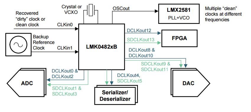
The LMK04821 family of devices provide a good case study for this topic because they are high-performance, dual-loop jitter cleaners that can drive up to seven JESD204B converters or logic devices in a subclass-1 clocking scheme with device and SYSREF clocks. Figure 1 is a high level block diagram of a typical JESD204B system with the LMK04821 family devices as clocking solution.
 Figure 1 Typical JEDEC JESD204B
Application Block Diagram
Figure 1 Typical JEDEC JESD204B
Application Block DiagramThe LMK04821 generates SYSREF signals with a single SYSREF clock divider from the voltage-controlled oscillator of the second phase-locked loop (PLL) . From the divider, the signal gets distributed to the individual output paths. Each output path contains digital and analog delays to adjust the SYSREF phase in relation to the device clock.
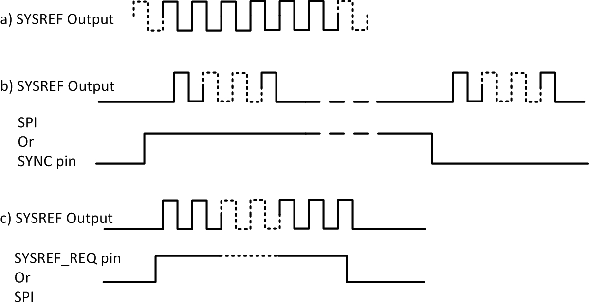
From the JESD204B standard, SYSREF can be in different modes, as shown in Figure 2. It can be a continuous (also known as periodic), gapped periodic or one-shot signal. The continuous and gapped-periodic SYSREF periods must be in an integer multiple of the local multiframe clock (LMFC) in order to avoid SYSREF pulses in the middle of a multiframe.
Continuous mode allows for continuous output. Many developers don’t use continuous mode due to crosstalk from SYSREF to the device clock. However, continuous mode enables the system developers to manually set up the correct deterministic-phase relationship between both signals. After the setup it can be changed to gapped-periodic SYSREF.
In gapped-periodic or one-shot modes, the output of the SYSREF clock divider is fed through a pulser to the output paths. The pulser gates the SYSREF signal and lets only a few pulses through. The pulse count can be set to one, two, four or eight pulses. Since there isn’t a periodic signal, the crosstalk from SYSREF to the device clock is minimized.
Another type of gapped-periodic SYSREF mode in the LMK0482x is the request mode, which outputs a continuous stream of SYSREF pulses as long as the SYNC/SYSREF_REQ pin is high.
 Figure 2 The SYSREF Modes of the
LMK0482x Are a) Continuous SYSREF, B) Pulsed SYSREF (One-shot or Gapped
Periodic), C) and SYSREF Request (Gapped Periodic)
Figure 2 The SYSREF Modes of the
LMK0482x Are a) Continuous SYSREF, B) Pulsed SYSREF (One-shot or Gapped
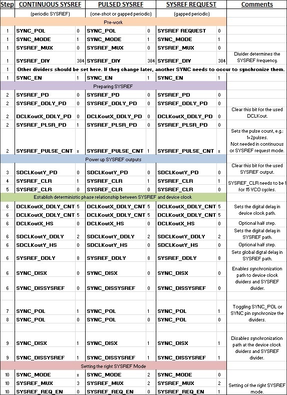
Periodic), C) and SYSREF Request (Gapped Periodic)In LMK04821 devices, the internal SYSREF distribution path is shared with the output-divider synchronization path. Therefore, it needs a specific register write sequence to enable synchronized outputs and glitch-free SYSREF pulse generation. In Figure 3, the methods I’ve described are listed with their register write sequences. Figure 3 also shows the internal-register field names with content as a decimal value. Steps with the same number are interchangeable.
 Figure 3 Register Write Sequences to
Enable Different SYSREF Modes
Figure 3 Register Write Sequences to
Enable Different SYSREF ModesThe JESD204B standard is reducing the layout efforts while introducing serialized data transmission between signal converters and logic devices. By taking full advantage of the SYSREF modes of your JESD204B-enabled clock device, you can easily create deterministic phase relationships in the whole system.
Are there other clock design challenges you’d like us to cover regarding JESD204B designs or others? Let me know by logging in to post a comment below.
Additional Resources
- Read the blog series about JESD204B subclasses.
- Read this blog post about JESD204B subclass-1 clocking timing requirements.
- Read this Analog Applications Journal article, “When is the JESD204B interface the right choice?”
- Get useful design tips on various clock and timing design challenges from the “Timing is Everything” blog series.