SSZTBJ7 march 2016 TPS53319 , TPS53355 , TPS53513 , TPS53515 , TPS53647 , UCD90240
A good power supply meets a specified performance level and isn’t heard from again. Not hearing back from your power supply means that it’s working as designed and there aren’t any problems.
But today, PMBus enables designers to continue communicating with their power supply, from development to characterization to field deployment. You can use the PMBus protocol standard’s robust command set to optimize your design in the development cycle. You can scale voltages and frequency to optimize processor power dissipation and data-center efficiency. You can work through sequencing schemes to optimize power up and power down. You can monitor the input/output voltage, current and power to improve reliability. A common use of PMBus is Adaptive Voltage Scaling (AVS) where the PMUs voltage regulator is commanded to output a different voltage, higher or lower, depending on the ASIC’s performance and temperature profile (Figure 1).
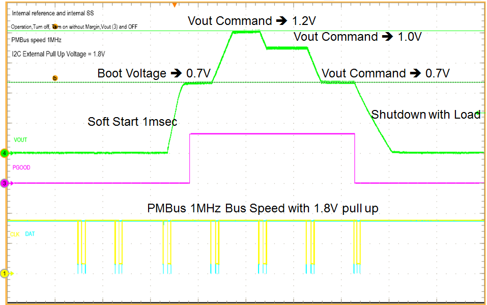 Figure 1 Output-voltage Adjustment
through PMBus
Figure 1 Output-voltage Adjustment
through PMBusOnce the design is complete, you can leverage PMBus in the qualification process, pushing the power supply to its limits by implementing voltage margining. Replacing the traditional external transistor and FET circuit, voltage margining stresses the output voltage independently up and down and defines the operating window, as seen in Figure 2.
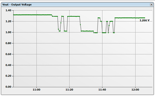 Figure 2 Output-voltage Margining
through PMBus
Figure 2 Output-voltage Margining
through PMBusIn production, you can configure fixed operating points for PMBus-enabled power supplies or set the supply to remain active and allow control from a master running PMBus scripts. A PMBus script is easy to put together with no programming experience. It’s like a flowchart with PMBus commands and their associated values put together from top to bottom.
The script flow as shown in Figure 3:
- First verifies the correct part present via the read DEVICE_CODE command.
- Writes the configuration (all the values you want to store into the integrated circuit [IC]) to the volatile memory of the IC via PMBus.
- Executes the PMBus STORE_XXX_ALL command to save the configuration to the IC’s nonvolatile memory (NVM).
- Resets the device power.
- Reads back the configuration via PMBus to confirm that the correct values were written to the IC.
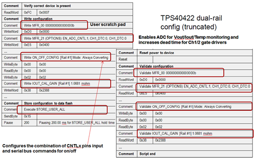 Figure 3 PMBus Manufacturing
Script
Figure 3 PMBus Manufacturing
ScriptAdaptive voltage scaling (AVS) is one of the functions most often implemented via PMBus. It enables on-the-fly output-voltage adjustment to optimize power dissipation and efficiency of the application-specific IC (ASIC) core rail. You can implement AVS through the standard VOUT_COMMAND in voltage regulators that have PMBus, or through analog voltage regulators managed by a PMBus manager such as the UCD90240. In Figure 4, the TPS53355, TPS53319, TPS53513 and TPS53515 are SWIFT™ analog integrated buck converters managed by the UCD90240. The UCD90240 can margin and change their output voltages.
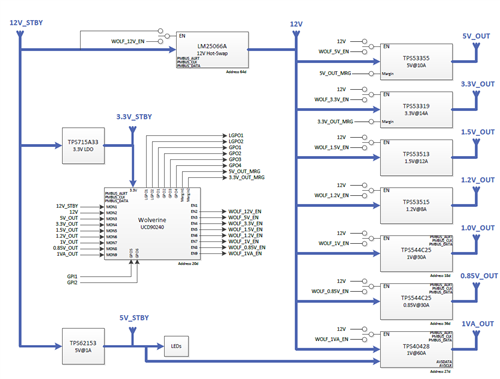 Figure 4 PMBus Power System with PMBus
Manager/sequencer and Analog and PMBus Voltage Regulators
Figure 4 PMBus Power System with PMBus
Manager/sequencer and Analog and PMBus Voltage RegulatorsOn an oscilloscope, the output-voltage change via PMBus looks like any voltage transition up or down, but it’s implemented via the PMBus digital serial protocol. Figure 5 shows the output voltage of a PMBus voltage regulator transitioning low as it’s commanded by the PMBus master (host processor, FPGA, ASIC) through the VOUT_COMMAND.
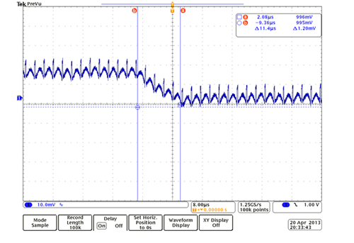 Figure 5 Output-voltage Change (AVS)
via the PMBus VOUT_COMMAND
Figure 5 Output-voltage Change (AVS)
via the PMBus VOUT_COMMANDOnce the end equipment is in the field, advanced PMBus telemetry can gather state-of-health information and aid in the debugging process with black-box capabilities. Through PMBus monitoring of input/output voltage, current, temperature and power, designers can enable load balancing in data centers, servers, switches and storage systems to optimize efficiency and increase reliability.
Figure 6 shows TI’s Fusion GUI Digital Power Designer Monitor screen where input/output voltage, current, power and temperature can be monitored real-time.
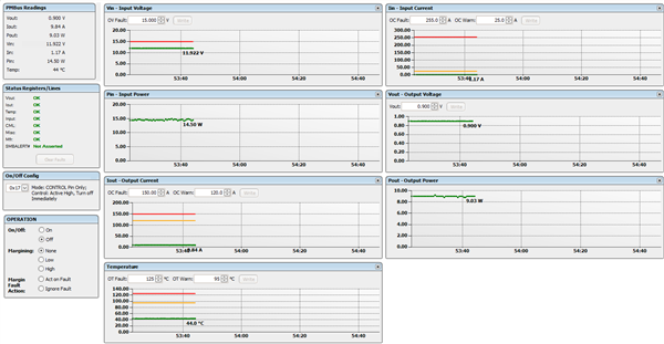 Figure 6 Input/output Voltage, Current,
Temperature and Power through TI’s PMBus Fusion Graphical User Interface (GUI)
(TPS53647 Example)
Figure 6 Input/output Voltage, Current,
Temperature and Power through TI’s PMBus Fusion Graphical User Interface (GUI)
(TPS53647 Example)So don’t say goodbye to your power supply. Just say “talk to you later.”
Additional Resources
- Consider the TPS53647 1/2/3/4-phase PMBus controller for your next design. Check out this project on WEBENCH® to start designing and optimizing your complete PoL DC/DC solution.
- Download a reference design and get started fast:
- “Complete PMBus Power System for Enterprise Ethernet Switches Reference Design” for three 3 ASIC/FPGA cores, DDR3 core memory, and auxiliary voltages found on high-performance Ethernet Switches.
- “High Density 4A DC-DC Buck Converter with PMBus Interface Reference Design” is a 1.8V 4A (3A without fan) for CPU I/O and other applications in a 22 cm by 12.5 cm single sided footprint.
- “12Vin Compact Dual 5V/5.5A Point-of-Load with PMBus using NexFET Power Block II Reference Design” is a compact dual 5.5A POL solution with PMBus in 0.65" by 0.90" siz
- Get more information on all of TI’s non-Isolated digital power solutions.