SSZTA25 July 2017 ADC12DJ3200 , LMK04828 , LMX2594
The JESD204B standard for data-converter clocking simplifies board routing, but puts some requirements on the device that clocks the data converter. One such requirement is the SysRef pulse that is sent to multiple data converters in order to mark a specific clock edge. The data converters use this pulse in order to line up their data streams. The SysRef pulse needs to occur away from the rising edges of the clock to ensure that it is clear to the data converter which edge it is marking.
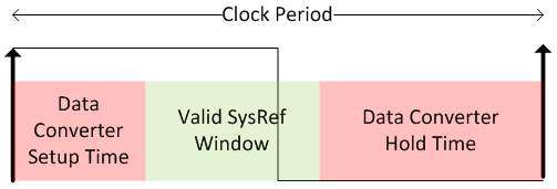 Figure 1 SysRef Pulse Edge
Placement
Figure 1 SysRef Pulse Edge
PlacementThe placement of this SysRef pulse becomes more challenging at higher clock frequencies as the period shortens. For instance, let’s say you were clocking multiple high-speed 9G-Hz digital-to-analog converters (DACs) with 50 ps setup and hold times. A 9-GHz clock has a period of 111 ps, so this only leaves a 11 ps window to place the SysRef. So you can see the challenge of precisely positioning the SysRef pulse for a high-frequency clock.
Single vs. Multiple Clocking Device Approach
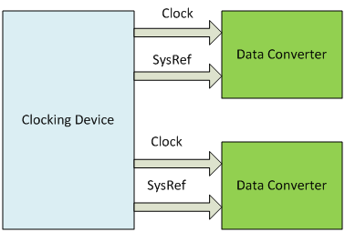 Figure 2 Single Clocking Device Approach
This method offers excellent control of the skew between SysRef and the clock, but it may be more challenging if the data converters are far from the clocking device and the clock is high frequency.
Figure 3 shows a multiple clocking device approach if the data converters are far apart and the traces are long. In this case, the skew between the re-clocked SysRef and high-frequency clock is better. The SysRef is sent from the master clocking device and retimed through the slave clocking device. This approach allows the high-frequency clock to have short traces and the re-clocked SysRef to have more precise control when the data converters are far apart on the board, or even on separate cards. There will be more skew between the clocks with this approach, but some devices allow you to adjust the skew and tune this out, and maintain the same adjustment settings between power-up cycles.
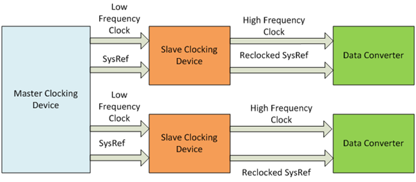 Figure 3 Multiple Clocking Device Approach
The Multi-Channel JESD204B 15GHz Clocking Reference Design for DSO, Radar and 5G Wireless Testers illustrates the multiple clocking device approach with the LMX2594. In this case, the LMK04828 is the master clocking device and the LMX2594 is the slave clock. The LMX2594 has a sync feature that enables consistent delay through the device, even through power cycles. The fact that the delay is consistent means that it’s correctable either in software or with the LMX2594’s global delay adjustment, which is also consistent even through power cycles. The LMX2594 enables you to adjust the SysRef delay with about 10ps resolution. Figure 4 shows the approach that was used.
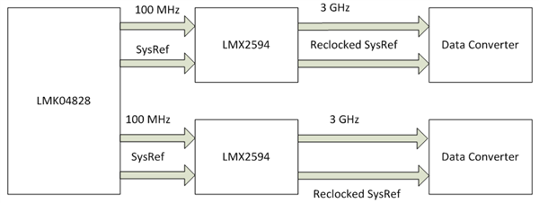 Figure 4 High-speed Clocking Example
Figure 5 shows two 3-GHz clocks generated from two LMX2594 devices. As you can see, both the devices and their corresponding SysRef signals are in alignment. You can use this setup for any clock frequency from 10 MHz to 15 GHz using the LMX2594.
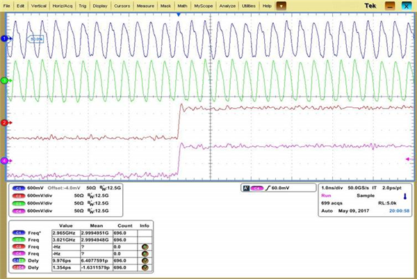 Figure 5 Measured Output
As JESD204B data converter clock rates increase, the timing of the SysRef pulse becomes more demanding and needs the clocking device to have fine delay adjustment. The choice of devices that can do this becomes more limited, but there are a few devices that can do this.
Additional Resources
- Read the technical article, “Timing is everything: JESD204B subclass 1 clocking timing requirements.”