SSZT259 august 2020 LM61460-Q1 , LMQ61460-Q1 , LMR33630-Q1 , LMR36015-Q1
As automotive systems continue to evolve, the number of applications requiring additional power continues to increase. Engineers designing higher-power systems often switch from low-dropout (LDO) regulators to DC/DC buck converters, given the latter’s improved efficiency and thermal performance. Unfortunately, making this switch comes at a cost, since DC/DC buck converters have considerably higher electromagnetic interference (EMI) than the LDO regulators they replace.
Because EMI can affect sensitive components such as the AM/FM radio receiver and driving-assist sensors, and because significant EMI can actually degrade or even prevent proper system operation, official standards like Comité International Spécial des Perturbations Radioélectriques (CISPR) 25 Class 5 set EMI limits for vehicles and boats with internal combustion engines.
Outsmarting board layout limitations
One of the easiest ways to mitigate EMI is with the right printed circuit board (PCB) layout. For a buck converter, your most important considerations are:
- Reducing the surface area of high transient voltage (dv/dt) nodes.
- Reducing the loop area of high transient current (di/dt) loops.
These considerations dictate the placement of certain components that, when done properly, can help minimize EMI.
A board’s size or shape can limit certain component placements, however, and the time and cost required to perform board spins may be prohibitive. So what are your options if you have such constraints but need to remain under CISPR 25 Class 5 EMI limits in your application?
If it’s not possible to optimize your layout for EMI, there are DC/DC converters with layout-agnostic package and feature improvements at the device level that can help mitigate EMI when an EMI-optimized layout isn’t an option.
EMI-friendly device-level features
Spread spectrum is a feature that dithers the switching frequency to spread the harmonic peaks of EMI caused by the switch node. Spreading the energy of the higher harmonic peaks turns tall, sharp emissions into low, smooth emissions, which in turn reduces the amount of filtering and optimization needed for a design to fall under emissions limits.
Slew-rate control reduces the turnon time of the high-side field-effect transistor (FET), which reduces energy in the high-frequency harmonics. Simply add a small resistor in series with the boot capacitor, or use a boot resistor on the dedicated RBOOT pin of devices that have this feature built-in. Slowing the slew of the FETs improves EMI but decreases efficiency, however.
EMI-friendly packages
Package-level features that can help suppress EMI include TI’s HotRod™ flip-chip-on-leadframe package, which has no internal bond wires; see Figure 1. Removing inductive bond wires in the path of the high di/dt loop of the input capacitors’ discontinuous current eliminates a significant source of input loop inductance and satisfies one of the primary considerations I mentioned earlier – reducing the area of high di/dt loops.
 Figure 1 Cross-section of a standard wire-bond quad flat no-lead package and a HotRod package
Another package-level feature is the use of a symmetrical pinout for critical paths. DC/DC buck converters such as the LMR33630-Q1, LMR36015-Q1, LM61460-Q1 and LMQ61460-Q1 have a switch-node pin in the center with PGND and VIN on either side.. Such symmetry creates magnetic fields that provide better field containment and reduce coupling to nearby circuits.
Integrated input capacitors
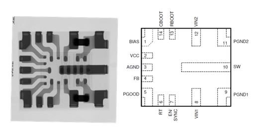
To mitigate EMI even further at the device level, products such as the LMQ61460-Q1 now integrate input capacitors inside the package. Figure 2(a) represents these capacitors as dark rectangles straddling upper- and lower-right pin pairs VIN and PGND. Refer to Figure 2(b) for the pinout. Including input capacitors inside the package reduces parasitic inductance, ringing and high-frequency EMI (again satisfying the second consideration). High-frequency EMI is particularly important because problems in the high-frequency range can become worse in the presence of higher input voltages and higher output currents – conditions common in automotive applications.
 Figure 2 X-ray image of the LMQ61460-Q1
with integrated capacitors (a); LMQ61460-Q1 pinout (b)
Figure 2 X-ray image of the LMQ61460-Q1
with integrated capacitors (a); LMQ61460-Q1 pinout (b)(a) (b)
EMI does present challenges in automotive applications. But board layout constraints don’t automatically mean that you’re out of options. Device-level features and modern package types offer reliable EMI mitigation techniques so that you can improve your designs and confidently remain under EMI emissions limits.
Additional resources
- To learn more about how packaging affects EMI, watch the training video, “Reduce EMI and shrink solution size with HotRod packaging.”
- Read the Analog Design Journal article, “Reduce buck-converter EMI and voltage stress by minimizing inductive parasitics.”
- For more information about optimizing automotive designs to meet EMI emissions limits, read the application report, “Reduce Conducted EMI in Automotive Buck Converter Applications.”