-
C2000 ADC (Type-3) Performance Versus ACQPS SPRACP5 December 2019 TMS320F2802-Q1 , TMS320F28020 , TMS320F280200 , TMS320F28021 , TMS320F28022 , TMS320F28022-Q1 , TMS320F280220 , TMS320F28023 , TMS320F28023-Q1 , TMS320F280230 , TMS320F28026 , TMS320F28026-Q1 , TMS320F28026F , TMS320F28027 , TMS320F28027-Q1 , TMS320F280270 , TMS320F28027F , TMS320F28027F-Q1 , TMS320F28030 , TMS320F28030-Q1 , TMS320F28031 , TMS320F28031-Q1 , TMS320F28032 , TMS320F28032-Q1 , TMS320F28033 , TMS320F28033-Q1 , TMS320F28034 , TMS320F28034-Q1 , TMS320F28035 , TMS320F28035-EP , TMS320F28035-Q1 , TMS320F28050 , TMS320F28051 , TMS320F28052 , TMS320F28052-Q1 , TMS320F28052F , TMS320F28052F-Q1 , TMS320F28052M , TMS320F28052M-Q1 , TMS320F28053 , TMS320F28054 , TMS320F28054-Q1 , TMS320F28054F , TMS320F28054F-Q1 , TMS320F28054M , TMS320F28054M-Q1 , TMS320F28055 , TMS320F2806-Q1 , TMS320F28062 , TMS320F28062-Q1 , TMS320F28062F , TMS320F28062F-Q1 , TMS320F28063 , TMS320F28064 , TMS320F28065 , TMS320F28066 , TMS320F28066-Q1 , TMS320F28067 , TMS320F28067-Q1 , TMS320F28068F , TMS320F28068M , TMS320F28069 , TMS320F28069-Q1 , TMS320F28069F , TMS320F28069F-Q1 , TMS320F28069M , TMS320F28069M-Q1
-
C2000 ADC (Type-3) Performance Versus ACQPS
C2000 ADC (Type-3) Performance Versus ACQPS
C2000™ ADC (Type-3) Performance Versus ACQPS
Analog-to-Digital Converters (ADCs) are an important part of the C2000 Microcontroller (MCU) devices. In embedded processing, the conversion of a real time signal into a digital reading is essential for many real-time applications. Often, choosing the correct setup and configuration for an ADC can be difficult depending on system requirements. This application report discusses configuration settings, specifically the acquisition sample and hold time (ACQPS), with a focus on the F2803x device family. Some insight is given into which ACQPS values should be avoided based on the internal structure of a type 3 ADC in order to maximize the ADC’s performance by minimizing offset/gain error and achieving better integral and differential linearity. To achieve these results, this document follows a methodical approach first going through error internal to the ADC itself then the error based on ADC performance specifications. The information provided in this application report is applicable to all C2000 devices with a type 3 ADC.
Trademarks
C2000 is a registered trademark of Texas Instruments.
All other trademarks are the property of their respective owners.
1 Introduction
The sample and hold time, otherwise known as the ‘sample window’ time, is the amount of time allotted to charging the internal sampling capacitor of an ADC. Some applications may require a longer or shorter time depending on the drive strength of the external connections along the signal path to the ADC pin. For the F2803x device, the acquisition sample and hold (S+H) window size is configured in the ADCSOCxCTL register, and set to a value represented by one less than the desired number of ADC clock cycles. For example, an ACQPS value set to 28 would indicate 29 ADC clock cycles. Since this value is in terms of ADC clock cycles, it is dependent on the ADC's operational frequency. The F2803x devices have two ADC frequency settings, SYSCLK and SYSCLK/2, configurable through the CLKDIV2EN bit field in the ADCCTL2 register. This usually translates to 60 MHz and 30 MHz, respectively. The conversion time is always 13 ADC clock cycles. Therefore, the total time to process a single conversion of an analog voltage is the sample time plus the conversion time. For specific examples on finding the total processing time, see the TMS320F2803x Technical Reference Manual (TRM).
A smaller ACQPS value allows for more ADC readings within a given time frame in comparison to a larger ACQPS value. However, choosing a smaller ACQPS value may not allow the settling time of the sampling capacitor to stabilize, possibly leading to inaccurate results. Having an insufficient ACQPS value could also lead to cross-talk within sequential readings. Therefore, choosing the correct ACQPS value for a given system design is an important decision. Included in the TRM is a generalized list of non-valid ACQPS values. These values lead to significant variation from the specifications defined in the TMS320F2803x Microcontrollers Data Sheet for ADC performance. Table 1 expands on information provided by the TRM to list valid ACQPS values based on the data acquired in this analysis; these values are optimal ACQPS values that lead to stable ADC operation under all conditions and whose conversion results meet data sheet specifications. Values referred to as non-valid throughout this document are those which fall outside the valid ranges.
Table 1. Valid ACQPS Values
| Frequency (MHz) | Overlap Mode | Non-Overlap Mode |
|---|---|---|
| ≤ 30 | {6-63} | {6-63} |
| > 30 & < 60 | {7-11, 21-24, 34-36, 47-50, 60-63} | {7-16, 21-29, 34-42, 47-55, 60-63} |
| 60 | {6-10, 12-14, 20-23, 25-27, 33-36, 38-40, 46-49, 51-53, 59-62} | {6-16, 18-29, 31-42, 44-45, 57-63} |
The ADC can operate in overlap mode. In this mode, ADC conversions occur at the same time a new voltage is being sampled. By comparison, in non-overlap mode the sample and conversion of the input signal occur sequentially. Since the ACQPS value determines the amount of acquisition and hold time, the distinction between overlap and non-overlap mode impacts the amount of conversions the ADC performs within an application. Thus, this report will analyze both modes independently from one another.
In order to bound the effect of the S+H time on the ADC’s performance, the data sheet minimum, typical, and maximum conditions for operational temperature and analog voltage (VDDA) are discussed within this report in conjunction with the ACQPS setting. Intermediate values of these parameters can be assumed to follow similar trends, but require in-depth analysis for specific system conditions. Efforts were made to ensure the data presented had adequate code spread. For more information regarding this topic, see Section ASection A.1.
NOTE
All values referenced from the TMS320F2803x Microcontrollers Data Sheet are taken from the time this report was publicized.
2 Offset Error
The offset error of an ADC can be defined as the deviation between the measured and ideal reading, in terms of Least Significant Bits (LSBs), when a 0 volt (V) input is applied to any of the input pins. Usually offset error is adjusted for by correcting it through the OFFTRIM bits in the ADCOFFSETTRIM register. For more detailed information regarding the process of reducing offset error, see the ADC Zero Offset Calibration section in the TMS320F2803x Technical Reference Manual (TRM). Each ACQPS setting needs to be trimmed differently, as each of the values leads to a different offset error under the same system conditions. Also, each start of conversion (SOC) channel can be configured to have a different ACQPS setting. If this is done in an application, then each channel should be calibrated separately.
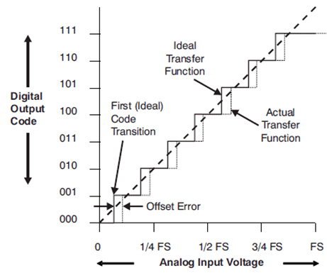
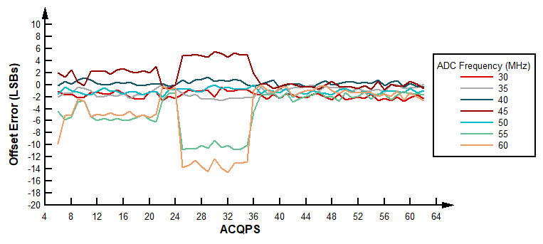
The data sheet specifies ± 20 LSBs of offset error after executing a single self-calibration and ± 4 LSBs for periodic self-recalibration. Figure 2 and Figure 3 show the variation of average offset error among different ACQPS values under nominal conditions with no calibration.
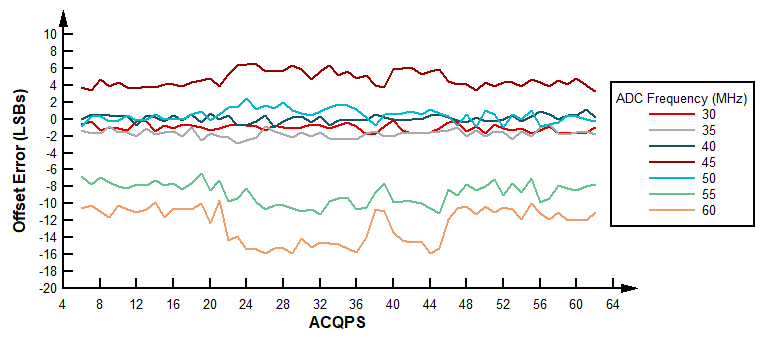
Specifically in overlap mode, there are certain ACQPS values that have worse offset error than others. Both in overlap and non-overlap mode, 60MHz can lead to larger negative offset errors particularity for non-valid ACQPS values. Errors from intermediate frequencies between 30 MHz and 60 MHz are not guaranteed to follow the same trends.
As the VDDA supply increases from the minimum supported value to the maximum, the offset error also increases, across non-valid ACQPS settings. The disparity between offset error as it correlates to frequency is also increased when the temperature is lowered to the minimum operational temperature. Therefore, the worst offset error is seen at the lowest operational temperature and the highest operational analog voltage.
As previously mentioned, the offset error can be corrected through calibration. Periodic self calibration is encouraged in order to reduce offset error due to fluctuations in temperature. For software examples on performing periodic self-calibration, or calibrating each SOC differently, see the ADC examples in C2000WARE.
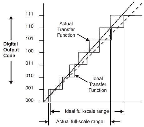
3 Gain Error
The gain error represents the deviation of the ADC’s actual transfer function to the ideal transfer function at the full scale range, maximum input voltage, after the offset error has been nullified. An ideal transfer function of an ADC is one in which the full scale range corresponds to the maximum output code. The F2803x devices have a 12 bit ADC with an internal reference of 3.3 V. For a resolution of 12 bits, the maximum digital output code is 4095. Therefore, in an ideal ADC, 3.3 V would map to a digital reading of 4095. The data sheet for this device family specifies that the gain error for the ADC is within ± 60 LSBs. Under these bounds, the ADC could interpret either 3.252 V (positive gain error) or a value up to 3.348 V (negative gain error) as the maximum output code reading instead of the full scale range. Positive gain error will saturate the converter at an earlier voltage reading; meaning all codes above a certain voltage threshold, depending on the amount of error, will result in the maximum output code.
NOTE
For the purpose of this analysis external reference mode was not considered.
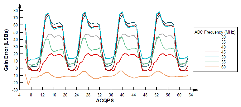
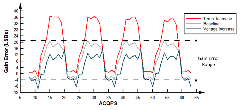
The gain error fluctuates in relation to ACQPS values when operating in overlap mode. Specifically referencing 30 and 60 MHz, as the operating temperature increases, the gain error range (maximum to minimum error value) also increases. 30 MHz is more susceptible to this change than 60 MHz. However, as temperature decreases, gain error becomes more dependent on the ADC operating frequency. This behavior causes some of the non-valid ACQPS values to have gain errors outside of the data sheet range.
An increase in voltage will shift the gain error down, towards larger negative values. This is however not applicable while operating at the lowest operable temperature because the error range does not shift with changes in VDDA.
Figure 6 shows these descriptions in a graphical form.
In non-overlap mode, input signals are only sampled while the ADC conversion stage is idle. Figure 7 illustrates how the gain error fluctuates in relation to ACQPS values when operating in non-overlap mode under nominal conditions. Much like overlap mode, the gain error range increases with increasing temperatures, solely in regards to 30 and 60 MHz; this shifted error range is still within the specified gain error range of ± 60 LSBs, as it is for all operable temperatures. Different values of VDDA will shift this range towards larger positive or negative gain errors depending on the operational frequency. For temperatures between the typical and maximum operable values, the larger VDDA voltages shift the gain error towards more negative values, as in overlap mode.
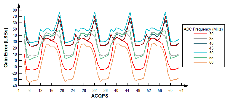
Based on the plots shown above, there are non-valid ACQPS values that have gain error that exceed those limits specified by the data sheet. In order to more closely model the ideal ADC transfer function, ACQPS values that have gain error outside of the data sheet specifications should be avoided as they can lead to an inaccurate representation of the full scale range.
4 Linearity Error
There are two forms of non-linearity: differential (DNL) and integral (INL). Both DNL and INL should be calculated when the gain and offset errors have been nullified in order to get an accurate representation for the ADC’s linearity performance.
4.1 Differential Non-Linearity Error
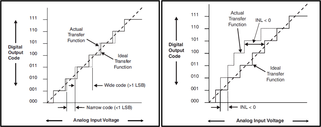
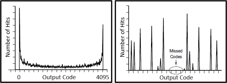
DNL error can be described as the difference in the output code width with regards to an ideal code width, which corresponds to 1 LSB. For the F2803x devices, the DNL error is categorized as ± 1 LSB for an ADC operating at 30 MHz or below. For higher frequencies there might be missing codes depending on the operational conditions (represented by a DNL value of -1). Missing codes indicate that one or more of the possible digital codes is never output. For more details on missing codes, see the TMS320F2803x MCUs Silicon Errata.
NOTE
For the purpose of this analysis, the histogram method was used to calculate the DNL error. For more information on this method, see Section B.
DNL can be represented by two values, the largest of the DNL errors found within all output codes, Max DNL, and the smallest, Min DNL. This report will discuss DNL in these terms for each ACQPS value.
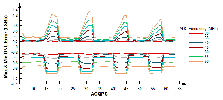
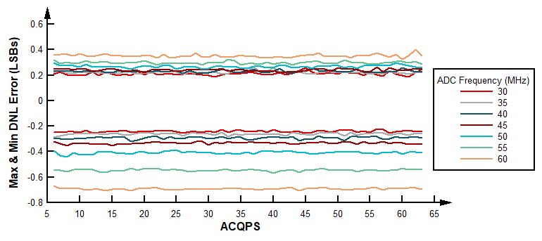
Both in overlap and non-overlap mode, operating the ADC at high frequencies and high temperatures causes larger bounds of error for Max and Min DNL. As can be seen in Figure 9 and Figure 10 there is less DNL error when operating at 30MHz. As the temperature is increased, the range of error between frequencies increases, in ascending order, ultimately leading to larger Max and Min DNL errors. Specifically in overlap mode, missing codes are seen for non-valid ACQPS values at high frequencies. Thus, the higher the frequency, the larger the chances become of missing an output code.
Better performance is seen with higher VDDA voltages. The disparity between error at different frequencies decreases, applicable across all temperatures. However, there are certain ACQPS values that are more susceptible to larger DNL error when VDDA is set to the lowest operational voltage. These effects are exasperated by higher ADC operational frequencies. For the susceptible ACQPS values at the lowest operable VDDA voltage, see Table 2.
Table 2. ACQPS Values Susceptible to High Linearity Error at Minimum VDDA
| Overlap Mode | Non-Overlap Mode |
|---|---|
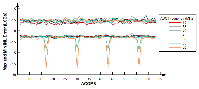
| {11, 24, 37, 50, 63} | {17, 30, 43, 56} |
4.2 Integral Non-Linearity Error
INL represents the deviation of the values on the ADC’s transfer function from the ideal. Each output code has an INL error that can be described as the summation of all DNL errors leading up that particular output code. The data sheet for the F2803x devices categorizes INL error to be within a ± 4 LSB range for an ADC operating at 30 MHz or below. Equation 1 is used to find the INL error of each output code.
In overlap mode, higher ADC frequencies result in a larger Max and Min INL error for non-valid ACQPS values, seen in Figure 11. The same type of curve applies at all tested temperatures and voltages. In the case of non-overlap mode, the INL error does not vary from operational conditions as much as in overlap mode. For both modes, the error is larger at higher temperatures than the nominal, 30 °C, when operating at higher ADC frequencies. This is applicable to all ACQPS values, but predominantly with the non-valid values. For more details on this subject, see the DC Specifications advisory within the TMS320F2803x MCUs Silicon Errata.
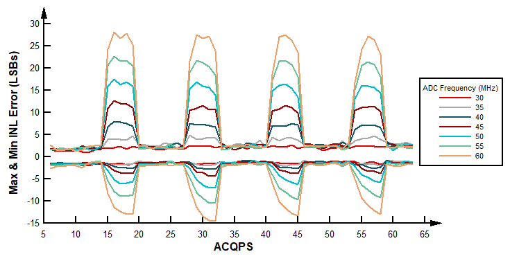
In regards to voltage conditions, performance does not vary with VDDA voltages for valid ACQPS values. However, for non-valid values the linearity error is minimized by decreasing the voltage. Note that when VDDA is set to the minimum value, Table 2 still applies. Figure 12 shows an example of these large spikes of INL error in non-overlap mode when VDDA is set to the minimum value for the ACQPS values not listed in Table 1.
5 Summary
This application report outlined the relationship between ACQPS values and ADC performance. More specifically, it explained the extent of error the valid and non-valid ACQPS values may have under different operational conditions. Based on the data presented through this document, non-valid ACQPS values will lead to an offset, gain, and/or linearity error outside the data sheet specifications due to the internal design of a type 3 ADC. ACQPS values categorized as non-valid for overlap and non-overlap modes should be avoided, and self-calibration should be performed in order to adhere to data sheet limits.
The parameters and settings discussed in this document will depend on the system design and configuration, but should be accounted for when trying to maximize the ADC's performance. Thus, in order to reduce the offset, gain, and linearity error with the valid ACQPS values an analog supply voltage between the typical and maximum values is desired as well as an operational temperature close to the typical value. The optimal ADC operating frequency to reduce error is 30 MHz, for which all ACQPS values are valid. Lastly, setting the ADC to operate in non-overlap mode will provide a larger set of ACQPS selection and reduce the risk of error.
6 References
- Texas Instruments: TMS320F2803x Microcontrollers Data Sheet
- Texas Instruments: TMS320F2803x Technical Reference Manual
- Texas Instruments: TMS320F2803x MCUs Silicon Errata
- TI Precision Labs - ADCs (https://training.ti.com/ti-precision-labs-adcs
- Texas Instruments: A Glossary of Analog-to-Digital Specifications and Performance Characteristics
- Texas Instruments:Understanding Data Converters
A DC Code Spread
A.1 Overview
In an ideal ADC, when a static input voltage is applied to a given ADC pin, the conversion of that input voltage is the same every time the signal is sampled and converted, regardless of the channel. Meaning that for a large sample set of the same input voltage, there should be no difference among conversions. However, more realistically, the conversion set can be modeled by a Gaussian plot. The closer the standard deviation of this plot is to zero the closer the system resembles an ideal ADC, as such the Signal to Noise Ratio (SNR) will improve, increasing the Effective Number of Bits (ENOB) there are to represent the ADC's full scale range. A high standard deviation will contribute additional error on top of inherent gain and linearity errors of the ADC. Thus, performing a code spread analysis is beneficial before evaluating the ADC’s performance in order to make sure there are no system issues that will affect the accuracy of the ADC's readings.
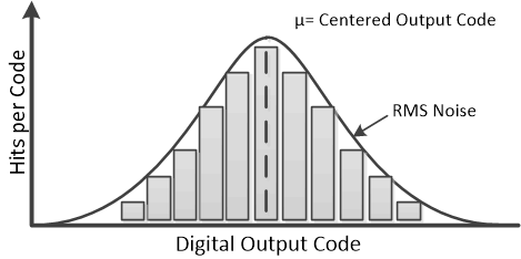 Figure 13. Code Spread
 A.2 Method
In order to perform a code spread analysis, it is important to know how much contribution there is from noise internal to the ADC. In order to quantify this, sample VREFLO, the low reference voltage, through ADC channel B5 and introduce an offset of approximately 30 LSBs. To set this internal connection write a 1 to the VREFLOCONV bit in the ADCCTL1 register. Then, calculate the standard deviation of the conversions; this will be the internal amount of deviation and should be taken as the baseline value.
Once there is a known baseline of code spread, incrementally add components to the signal path. For each, measure the amount of standard deviation from the resultant conversions. Subtract the acquired value from the baseline; this is how much deviation each of the added components contributes to the overall deviation. The reason this is compartmentalized is to potentially isolate different parts of the signal path and quantify each of their contributions. The goal is to try to minimize this value as much as possible so that there is little to no added system deviation from that of the baseline (internal code deviation). Verifying this ensures that the signal path does not introduce noise prior to the ADC conversion and thus lead to higher efficiency.
Possible ways to reduce code spread are ensuring the system has a low noise level and the input signal is as clean and reproducible as possible. Adding a low pass filter to the signal path will help remove high frequency noise and interference. The time constant of the filter depends on the sampling speed and the application requirements. Another best practice is adding buffering amplifiers between stages in the signal chain to ensure impedance matching.
B Calculating DNL Error
B.1 Histogram Method
This section explains in greater detail how the histogram method is used to calculate DNL error. In this method, a sine wave or ramp function is delivered to the ADC pin. This signal may be filtered or altered to meet additional system requirements and ensure a clean input signal. The ADC should be configured to constantly sample the input signal as the function is swept. After every conversion, a tally is kept corresponding to a certain digital output code; each code represented by a bin. Every time a conversion matches one of the codes, referred to a ‘hit’, the tally for that digital output code is increased by one. Ideally, after one complete period of the input function the tallies for each output code, width size, should be the same indicating no DNL error.
The minimum and maximum output codes are discarded from this analysis since they will skew the data with large number of hits unless the input function is perfectly timed to start and end along with the ADC. Beginning with the first bin, second output code, the DNL error is found using Equation 2; here 'Average Hits' signifies the average number of hits for all the bins excluding those that correspond to the minimum and maximum output codes for the reason previously mentioned.
A positive DNL error, larger # of hits than the average, signifies that the respective output code will represent a wider range of voltage than that of 1 LSB. Whereas, a negative DNL error, smaller # of hits than the average, indicates the opposite. For a visual reference, see Figure 14.
IMPORTANT NOTICE AND DISCLAIMER
| TI PROVIDES TECHNICAL AND RELIABILITY DATA (INCLUDING DATASHEETS), DESIGN RESOURCES (INCLUDING REFERENCE DESIGNS), APPLICATION OR OTHER DESIGN ADVICE, WEB TOOLS, SAFETY INFORMATION, AND OTHER RESOURCES “AS IS” AND WITH ALL FAULTS, AND DISCLAIMS ALL WARRANTIES, EXPRESS AND IMPLIED, INCLUDING WITHOUT LIMITATION ANY IMPLIED WARRANTIES OF MERCHANTABILITY, FITNESS FOR A PARTICULAR PURPOSE OR NON-INFRINGEMENT OF THIRD PARTY INTELLECTUAL PROPERTY RIGHTS. |
| These resources are intended for skilled developers designing with TI products. You are solely responsible for (1) selecting the appropriate TI products for your application, (2) designing, validating and testing your application, and (3) ensuring your application meets applicable standards, and any other safety, security, or other requirements. These resources are subject to change without notice. TI grants you permission to use these resources only for development of an application that uses the TI products described in the resource. Other reproduction and display of these resources is prohibited. No license is granted to any other TI intellectual property right or to any third party intellectual property right. TI disclaims responsibility for, and you will fully indemnify TI and its representatives against, any claims, damages, costs, losses, and liabilities arising out of your use of these resources. |
| TI’s products are provided subject to TI’s Terms of Sale (www.ti.com/legal/termsofsale.html) or other applicable terms available either on ti.com or provided in conjunction with such TI products. TI’s provision of these resources does not expand or otherwise alter TI’s applicable warranties or warranty disclaimers for TI products. |
| Mailing Address: Texas Instruments, Post Office Box 655303, Dallas, Texas 75265
Copyright © 2019, Texas Instruments Incorporated |