SNVU651 January 2019
7 Board Layout
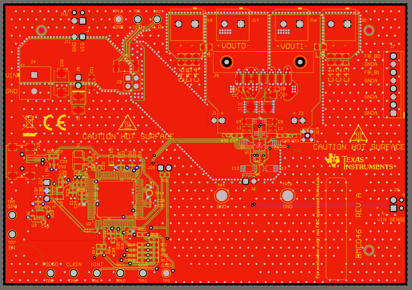
This section describes the board layout of the TPS65653-Q1. See the TPS65653 data sheet for specific PCB layout recommendations. The board is constructed on a 4-layer PCB. Figure 4 shows the top view of the entire board. Routing is mostly done on top and bottom layers. Top layer contains the copper areas connecting the VOUT pads of the inductors and output capacitors together and to the load terminals. 2nd layer is the ground plane and 3rd layer contains the VIN copper area and copper areas for the VOUT nets. Also the bottom layer contains large copper area filled with ground. Input capacitors are placed as close as possible to the TPS65653 device for keeping the critical VIN and GND traces short. Output capacitors and inductors are placed around the input capacitors.
 Figure 4. TPS65653-Q1 Board Layout