SNOAA78 June 2021 DS26F31MQML-SP , DS26F32MQML-SP
Measurement Results
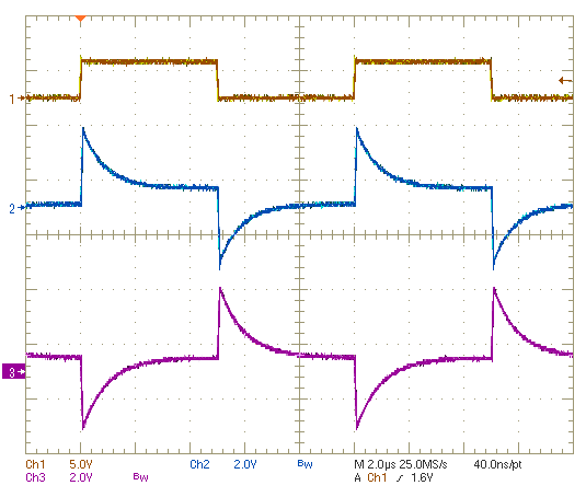
RS-422-based circuit
The following scope plot shows the input and output signals measured directly at the receiver input pins after transmission over a 5-m length of 24-AWG twisted-pair cable. Channel 1 shows the driver input signal and channels 2 and 3 the positive and negative inputs of the differential receiver. The hysteresis generated at the positive input of the receiver can be seen in the different quiescent levels to which the input returns after the initial capacitive "kick". In contrast, the inverting input, which does not have hysteresis, returns to the same quiescent level. This approach ensures that the receiver output remains in the last state to which it was driven and that the minimum switching frequency is independent of the time constant of the AC-coupling components.