SLVU642A May 2012 – August 2021 TPS54526
5.1 Layout
The board layout for the TPS54526EVM-608 is shown in Figure 5-1 through Figure 5-6. The top layer contains the main power traces for VIN, VO, and ground, and connections for the pins of the TPS54526 and a large area filled with ground. Many of the signal traces are also located on the top side. The input decoupling capacitor are located as close to the IC as possible. The input and output connectors, test points, and most of the components are located on the top side. R3, the 0-Ω resistor that connects VIN to VCC and R4, and the power good pullup are located on the back side. Analog ground and power ground are connected at a single point on the top layer near pin 5 of the TPS54526. The internal layer 1 is a split plane containing analog and power grounds. The internal layer 2 is primarily power ground. There are also a fill area of VIN and a trace routing VCC to the enable control jumper JP1. The bottom layer is primarily analog ground. There are also traces to connect VIN to VCC through R3, traces for the power good signal, and the feedback trace from VOUT to the voltage setpoint divider network.
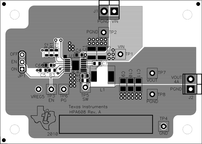 Figure 5-1 Top Assembly
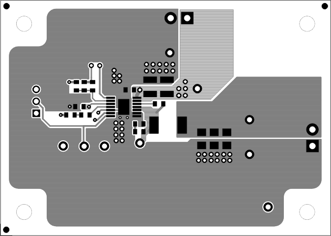 Figure 5-2 Top Layer
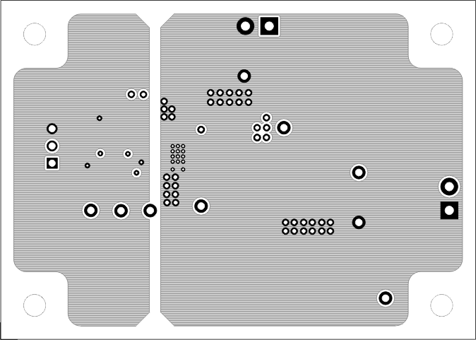 Figure 5-3 Internal Layer 1
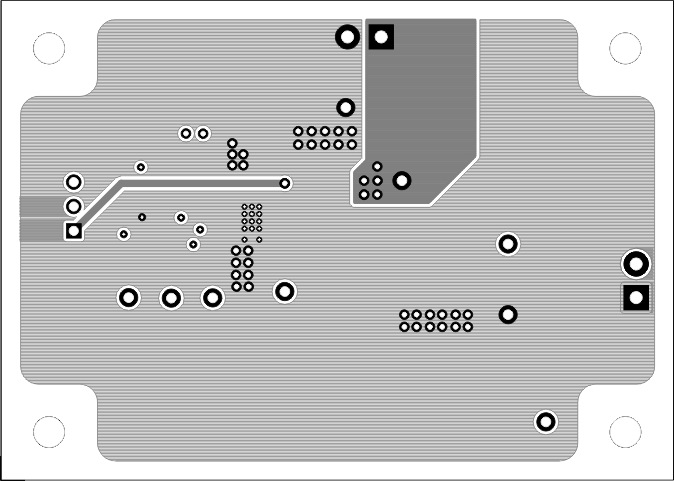 Figure 5-4 Internal Layer 2
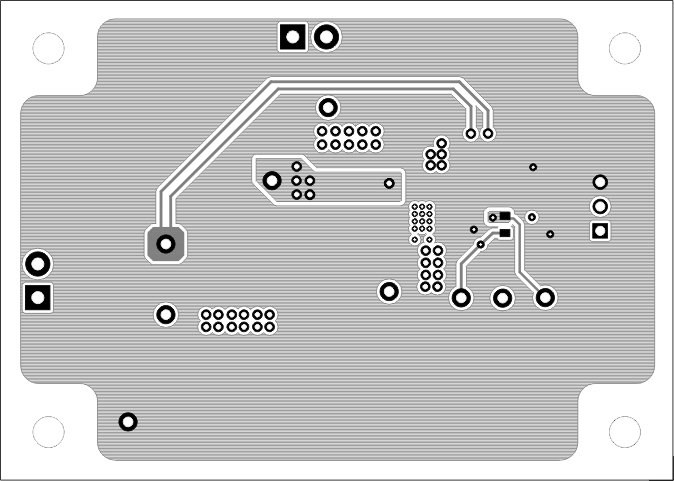 Figure 5-5 Bottom Layer as Seen from Back Side
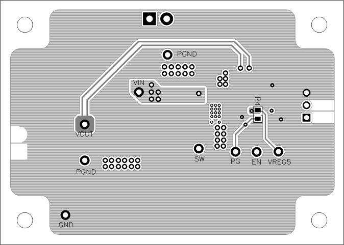 Figure 5-6 Bottom Assembly as Seen from Back Side