SLUU943A May   2012  – December 2021 TPS53014


  1. Introduction
  2. Description
    1. 2.1 Typical Applications
    2. 2.2 Features
  3. Electrical Performance Specifications
  4. Schematic
  5. Test Setup
    1. 5.1 Test Equipment
    2. 5.2 Recommended Test Setup
  6. Configurations
    1. 6.1 Enable/Disable Switch S1
  7. Test Procedure
    1. 7.1 Line/Load Regulation and Efficiency Measurement Procedure
    2. 7.2 List of Test Points
    3. 7.3 Equipment Shutdown
  8. Performance Data and Typical Characteristic Curves
    1. 8.1 Efficiency
    2. 8.2 Load Regulation
    3. 8.3 Line Regulation
    4. 8.4 Load Transient
    5. 8.5 Output Ripple
    6. 8.6 Switching Node
    7. 8.7 Enable Start-Up
    8. 8.8 Disable
    9. 8.9 Thermal Image
  9. EVM Assembly Drawing and PCB Layout
  10. 10List of Materials
  11. 11Revision History

EVM Assembly Drawing and PCB Layout

The following figures (Figure 9-1 through Figure 9-5) show the design of the TPS53014EVM-126 printed circuit board. The EVM has been designed using a 4-layer, 2-ounce copper circuit board.
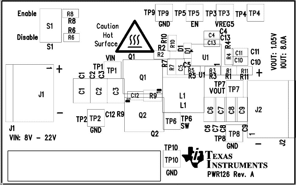
GUID-EB340889-8DD9-4659-89BD-88425A94EF0C-low.gifFigure 9-1 TPS53014EVM-126 Top Layer Assembly Drawing (Top View)
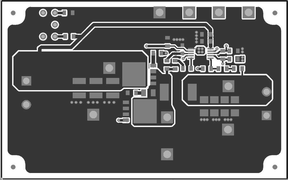
GUID-DCDAC9B6-4BE2-48F3-B692-B46214E25FEE-low.gifFigure 9-2 TPS53014EVM-126 Top Copper (Top View)
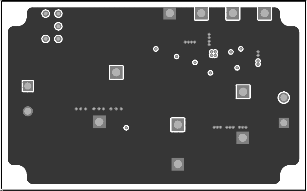
GUID-639AE4BB-FCB8-4DEB-970A-52577EDF086F-low.gifFigure 9-3 TPS53014EVM-126 Layer 2 (Top View)
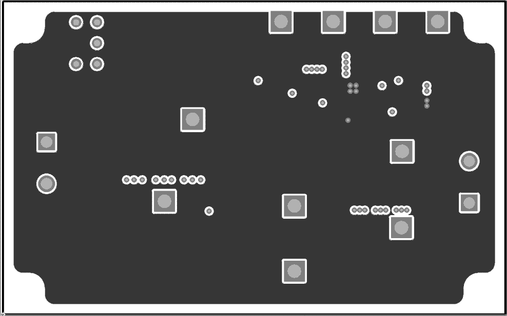
GUID-72A8078C-B6C5-419A-A3B3-961C22A58A15-low.gifFigure 9-4 TPS53014EVM-126 Layer 3 (Top View)
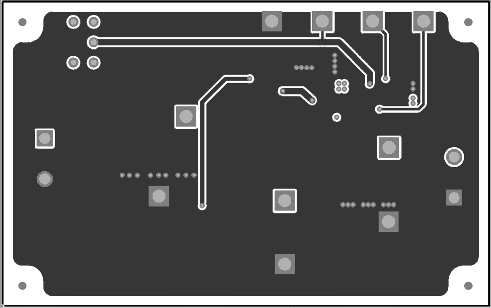
GUID-6BE6E112-B245-401D-ACB3-B8B9D6695836-low.gifFigure 9-5 TPS53014EVM-126 Bottom Layer (Top View)