SLLU149E June 2011 – February 2016 TUSB7320 , TUSB7340
- TUSB73x0 Board Design and Layout Guidelines
- 1 Typical System Implementation
- 2 Power
- 3 Device Reset
- 4 General High Speed Layout Guidelines
- 5 USB Connection
- 6 Package and Breakout
- 7 PCI Express Connection
- 8 Wake from S3
- 9 Device Input Clock
- 10JTAG Interface
- 11Differential Pair ESD Protection
- 12SuperSpeed Redriver
- 13SMI Pin Implementation
- 14Schematics
- Revision History
3.1 Overview
There is no GRST# timing constraint with respect to the power supplies, other than it should not be deasserted until the power supplies are stable.
However, extreme care must be taken if a passive reset is used, such as using the internal GRST# pull up or an external RC circuit, to ensure that the GRST# does not deassert until the 3.3-V and 1.1-V rails are within 10% of nominal. If the 3.3-V power ramps before the 1.1-V supply, and GRST# is deasserted, the device I/O is in an undefined state before the core logic is active. This allows the potential for the GRST# I/O cell to incorrectly configure as an output and drive the GRST# signal high until the core logic is powered on and correctly configures the cell.
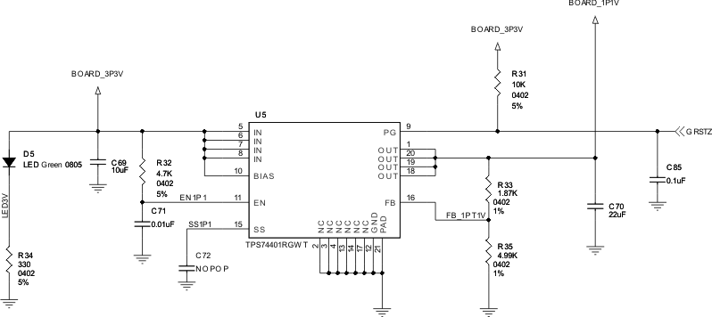
It is highly recommended that the GRST# input be connected to a power good output from a power supply to ensure that it does not deassert until both the 3.3-V and 1.1-V power rails are within 10% of their nominal value. The recommended sequence is to have the 3.3-V feed a 1.1-V regulator and then use the 1.1-V Power Good signal to drive GRST# as outlined below.
 Figure 3-1 1.1-V Regulator