SLAA126B April 2001 – September 2018 MSP430F149 , MSP430F149 , TLC3544 , TLC3544 , TLC3548 , TLC3548
5.2 Operating the ADC
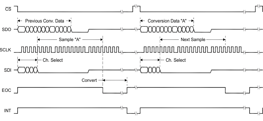
This application report is based on the one-shot operating mode (mode 00) using chip select (CS) as a conversion trigger. In this mode, each cycle performs one sample and one conversion on the selected analog input channel. Operation begins by bringing chip select low.
Channel selection is accomplished by writing 0000h through 0700h to the SDI pin of the ADC. The microprocessor presented in this application report uses 8-bit data packets when writing to the serial port. The upper and lower bytes are transmitted to the ADC by writing to the micro’s data buffer twice, while holding the CS pin low. The first byte [D15:D8] contains the channel selection information, and the second byte [D7:D0] consists of zeros, or a dummy value transfer.
The TLC3544 and TLC3548 also feature three test modes that can be accessed by writing 0xB000h, 0xC000h or 0xD000h to the SDI pin. Test mode 1 (0xB000h) presents a digital code on SDO equivalent to (REFP + REFM) / 2. Test mode 2 and 3 present a digital code equal to REFM or REFP respectively.
 Figure 3. Sample-and-Convert Cycle