This section provides a failure mode analysis
(FMA) for the pins of the TLVH431B-Q1 (DBV and DBZ
package). The failure modes covered in this document include the typical pin-by-pin
failure scenarios:
Table 4-2 through Table 4-9 also indicate how these pin conditions can affect the device as per the failure
effects classification in Table 4-1 .
Table 4-1 TI Classification of Failure
Effects CLASS FAILURE EFFECTS A Potential device damage that affects
functionality B No device damage, but loss of functionality C No device damage, but performance degradation D No device damage, no impact to functionality or
performance
Figure 4-1 shows the TLVH431B-Q1 pin diagram for the DBV package. For a description of the device
pins, see the TLVH431B-Q1 datasheet .
Figure 4-1 Pin Diagram (DBV ) Package
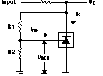
CATHODE is connected to VDD through a series resistor
ANODE is connected to the ground
REF is connected to ground and cathode via resistors as shown in the Figure 4-2
NC and * pin is left floating
Figure 4-3 shows the
TLVH431B-Q1 pin diagram for the DBZ package. For a description of the device pins, see the
the TLVH431B-Q1 datasheet .
Figure 4-3 Pin Diagram (DBZ ) Package
Following are the assumptions of use
and the device configuration assumed for the pin FMA in this section:
CATHODE is connected to VDD
through a series resistor ANODE is connected to the
ground REF is connected to ground and
cathode via resistors as shown in the Figure 4-4 Table 4-2 Pin FMA for Device Pins Short-Circuited to
Ground on DBV Package PIN NAME PIN NUM. DESCRIPTION OF POTENTIAL FAILURE EFFECT(S) FAILURE EFFECT CLASS
NC
1
Normal Operation
D
*
2
Works fine when anode is connected to Ground but can affect
application functionality otherwise
C
CATHODE
3
Potential damage to the device depending on the location of the
short. Shorts output voltage to ground, increases system
current
A
REF
4
Turns off the regulator. No damage to device but can affect
application functionality
B
ANODE
5
Works fine when anode is connected to Ground but
can affect application functionality otherwise
C
Table 4-3 Pin FMA for Device Pins Short-Circuited to Ground on DBZ Package
PIN NAME
PIN NUM.
DESCRIPTION OF POTENTIAL FAILURE EFFECT(S)
FAILURE EFFECT CLASS
REF
1
Turns off the regulator. No damage to device but can affect
application functionality
B
CATHODE
2
Potential damage to the device depending on the location of the
short. Shorts output voltage to ground, increases system
current
A
ANODE
3
Works fine when anode is connected to Ground but
can affect application functionality otherwise
C
Table 4-4 Pin FMA for Device Pins Open-Circuited on DBV
Package
PIN NAME
PIN NUM.
DESCRIPTION OF POTENTIAL FAILURE EFFECT(S)
FAILURE EFFECT CLASS
NC
1
Normal Operation
D
*
2
Normal Operation
D
CATHODE
3
No damage to device but can affect application
functionality
C
REF
4
No damage to device but can affect application
functionality
C
ANODE
5
No damage to device but can affect application
functionality
C
Table 4-5 Pin FMA for Device Pins Open-Circuited on DBZ Package
PIN NAME
PIN NUM.
DESCRIPTION OF POTENTIAL FAILURE EFFECT(S)
FAILURE EFFECT CLASS
REF
1
No damage to device but can affect application
functionality
C
CATHODE
2
No damage to device but can affect application
functionality
C
ANODE
3
No damage to device but can affect application
functionality
C
Table 4-6 Pin FMA for Device Pins
Short-Circuited to Adjacent Pin on DBV Package
PIN NAME
PIN NUM.
SHORTED TO
DESCRIPTION OF POTENTIAL FAILURE EFFECT(S)
FAILURE EFFECT CLASS
NC
1
*
Normal Operation
D
*
2
CATHODE
Potential damage to the device depending on the location of the
short. Shorts output voltage to ground, increases system
current
A
CATHODE
3
REF
Works fine when used in REF to CATHODE direct feedback but can
affect application functionality otherwise
C
REF
4
ANODE
Turns off the regulator. No damage to device but can affect
application functionality
B
ANODE
5
NC
Normal Operation
D
Table 4-7 Pin FMA for Device Pins Short-Circuited to Adjacent Pin on DBZ
Package
PIN NAME
PIN NUM.
SHORTED TO
DESCRIPTION OF POTENTIAL FAILURE EFFECT(S)
FAILURE EFFECT CLASS
REF
1
CATHODE
Works fine when used in REF to CATHODE direct feedback but can
affect application functionality otherwise
C
CATHODE
2
ANODE
Potential damage to the device depending on the location of the
short. Shorts output voltage to ground, increases system
current
B
ANODE
3
REF
Turns off the regulator. No damage to device but
can affect application functionality
B
Table 4-8 Pin FMA for Device Pins Short-Circuited to
Cathode on DBV
Package
PIN NAME
PIN NUM.
DESCRIPTION OF POTENTIAL FAILURE EFFECT(S)
FAILURE EFFECT CLASS
NC
1
Normal Operation
D
*
2
Potential damage to the device depending on the location of the
short. Shorts output voltage to ground, increases system
current
A
CATHODE
3
Normal Operation
D
REF
4
Works fine when used in REF to CATHODE direct feedback but can
affect application functionality otherwise
C
ANODE
5
Potential damage to the device depending on the
location of the short. Shorts output voltage to ground, increases
system current
A
Table 4-9 Pin FMA for Device Pins Short-Circuited to Cathode on DBZ
Package
PIN NAME
PIN NUM.
DESCRIPTION OF POTENTIAL FAILURE EFFECT(S)
FAILURE EFFECT CLASS
REF
1
Works fine when used in REF to CATHODE direct feedback but can
affect application functionality otherwise
C
CATHODE
2
Normal Operation
D
ANODE
3
Potential damage to the device depending on the
location of the short. Shorts output voltage to ground, increases
system current
A
 Figure 4-2 Test Circuit for VKA > VREF
 Figure 4-4 Test Circuit for
VKA > VREF