SBOA510 March 2021 OPA455 , OPA462
- Trademarks
- 1Introduction
- 2Three Op Amp OPA462 HV Solution
- 3Lower Voltage, Lower Cost Three Op Amp Solution
- 4OPA462 300 Vpp Output Solution With Discrete Transistor Supply-Rail Drivers
- 5Lessons Learned from the Practical Implementation of the HV Op Amp Solutions
-
A Appendix
- A.1 Overview
- A.2 Summary of Results
- A.3 Test Setup and Equipment
- A.4 Printed Circuit Boards
- A.5 Power Supply, Source Measurement Unit (SMU)
- A.6 Arbitrary Waveform Generator (AWG)
- A.7 Oscilloscope
- A.8 Circuit 1: OPA462 Three op amp Solution
- A.9 Circuit 2: Lower Voltage, Lower Cost Three Op Amp Solution
- A.10 Circuit 3: OPA462 300 Vpp Output Solution With Discrete Transistor Supply-Rail Drivers
3 Lower Voltage, Lower Cost Three Op Amp Solution
Many op amp designs are not only performance demanding, but cost sensitive as well. That balance was an important consideration for the next OPA462 HV amplifier design. If the maximum supply-voltage range required for U1 can be limited to a maximum of 220 V, a lower cost solution can be realized compared to the three OPA462 solution.
This next design also employs a three op amp bootstrap circuit, but substitutes a lower voltage OPA196 or OPA990 op amp in the U2 and U3 positions formerly held by the two OPA462 HV op amps. These lower voltage op amps provide high DC precision, and offers lower cost compared to when three OPA462 HV op amps are used. The result is a HV amplifier whose maximum output voltage swing is increased by about 30 V to 35 V over that of a circuit using a single OPA462. The HV output capability is about 200 Vpp with a 25-mA load current and ±105-V (210 V) supplies. The actual output swing range will be dependent on the output load current being demanded as is the case with all op amps.
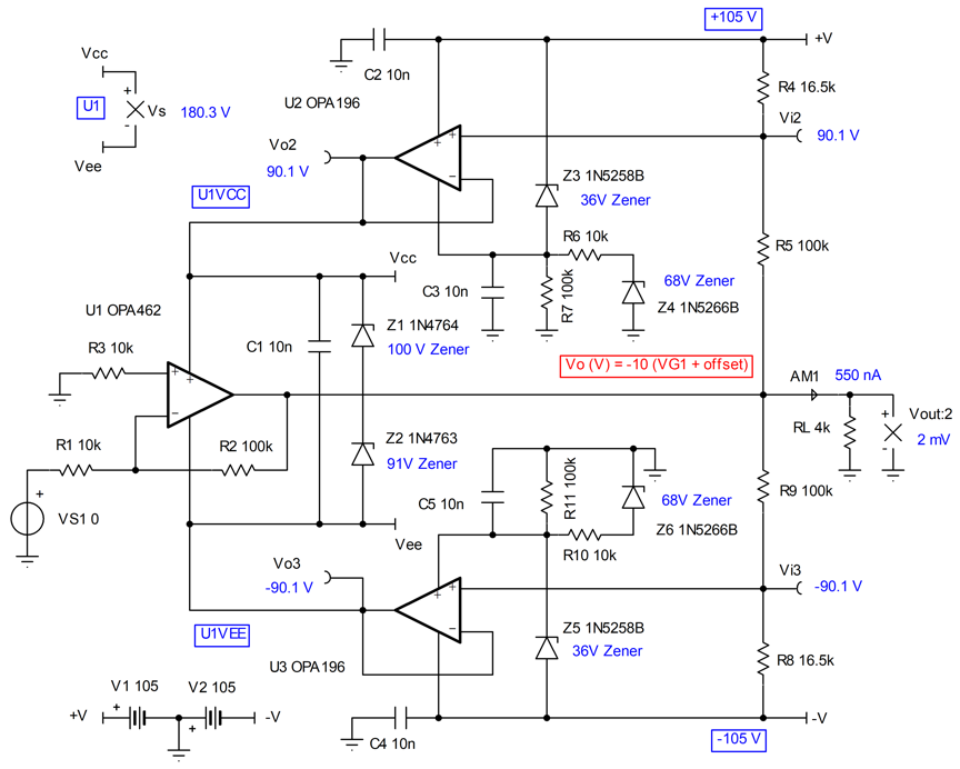
Figure 3-1 shows the circuit schematic for this second three op amp HV amplifier design. This amplifier is connected in an inverting amplifier configuration to demonstrate that these bootstrap circuits can be connected as either a non-inverting, or an inverting amplifier.
U1, an OPA462, is again the signal path amplifier as in the first three op amp HV circuit presented. A lower voltage OPA196, or the OPA990 op amps, are used in the U2 and U3 positions to drive the supply rail pins of U1. The circuit functions in the same manner as the first circuit does, but there are significant differences in the voltage levels developed at key circuit points compared to them in the three OPA462 HV circuit.
A goal for the circuit is to achieve a 200 Vpp output swing, without exceeding the OPA462 absolute maximum 190-V supply rating and 40-V rating for the OPA196 (42 V for OPA990). This goal can be achieved with the power supplies set to ±105 V by careful circuit planning. The supplies can be increased a bit higher as was done in the circuit presented in Section A. However, it is always a best practice to keep the voltage across the U1 several volts below the 190 V maximum to ensure a margin of safety.
 Figure 3-1 200 Vpp Output Solution
Achieved by Applying Lower Voltage Op Amps at the U2 and U3 Positions
 Similar to the circuits shown in Figure 2-1 and Figure 2-3, a voltage divider is connected from the U1 output to each of the +V and –V power supplies, which are set to +105 V and –105 V, respectively. In this case instead of the dividers establishing a voltage one-half the difference between the supply rail and the U1 output Vo1 level, they establish the voltage across the supply pins of U1 at 180 V. This is evident from schematic points Vi2 and Vi3 which are at +90 V and –90 V, respectively, when the U1 input is at 0 V.
U2 and U3 are configured as buffer amplifiers each having a gain of +1 V/V and the voltage dividers R4, R5 and R8, R9 establish the gain in each current path leading to the supply pins of U1. A gain of 0.14 V/V is established by the divider resistor values shown in Figure 3-1. Additionally, the gain can be determined by dividing the U2 or U3 full output swing voltage by the full U1 output swing required. When the U1 output swings 200 Vpp, U2 and U3 each have an output swing of 28 Vpp confirming the gain of 0.14 V/V.
The supply voltage for U2 and U3 are each established close to 36 V by the 36-V Zener diodes Z3 and Z5. The 10-kΩ R6 and R10 resistors, and 68-V Z4 and Z6 Zener diodes, provide supply current return paths for U2 and U3.
The Zener and resistor combinations shown in Figure 3-1 provide well-behaved power-up and power-down of the amplifier circuit. It is recommended that low-tolerance Zeners be employed where possible to help set the voltages close to ideal. Five-percent-tolerance Zeners have been available for many decades, and now 2% are common today and are preferred to establish the more critical circuit voltages. Adjustment of R6, R10 and the Z4, Z6 Zener voltage likely would be required if different supply voltages are used. Zener diodes Z1 (100 V) and Z2 (91 V) are added in series with each other and are connected across U1 to provide overvoltage protection.
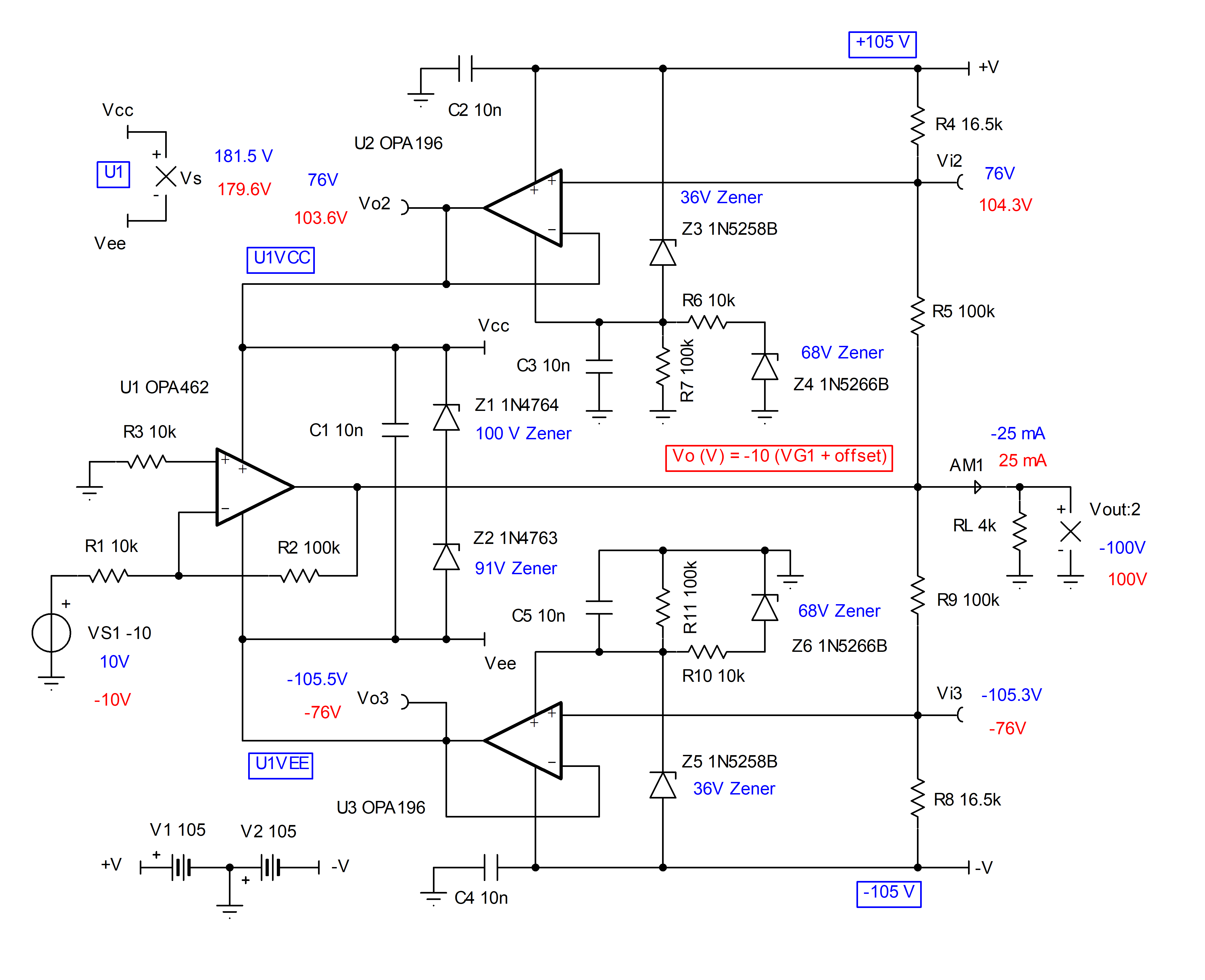
Figure 3-2 shows how the node voltages move and track as the input voltage is first set to +10 V (blue voltages), and then to –10 V (red voltages). Remember the OPA462 was configured as an inverting amplifier and that is the reason why the output voltage moves opposite to the input polarity.
When considering op amps for U2 and U3 be aware they provide both the DC and AC currents required by U1. That is to say, the DC operating current and any AC current of U1 demanded when driving RL will be sourced from U2 and U3, and thus these drivers must be capable of supplying that current. Any offset, offset drift, or other normal DC errors associated with U2 and U3 will be visible as a small error in the supply levels applied to U1. As a percentage of the supply voltage level, the error will be small.
Additionally, the lab tests performed with U2 and U3 as either the OPA462 or OPA196 indicated improved large-signal dynamic performance may be observed with this configuration, compared to just an OPA462 operating alone. This improvement is attributable to the inputs, outputs and supplies tracking each other across the output swing range. When that is the case, less current is needed to charge internal capacitances, and enhanced slewing performance can result.
 Figure 3-2 OPA462 HV + OPA196 Solution With
Input Voltages of +10 V (Blue) and –10 V (Red)
 A point to keep in mind with this three op amp circuit is that the U2 and U3 op amps must be individual op amps, and not the dual versions. U2 and U3 need to be electrically isolated from each other and cannot share a common substrate as a dual op amp does. Each requires its own separate power supply pins as the schematics indicate. Therefore, the OPA2196 and OPA2990 cannot be used here.