SBAU279 October   2020 ADS7038-Q1


  1.   Trademarks
  2. 1Introduction
  3. 2ADS7038Q1EVM-PDK Overview
    1. 2.1 Connections to Input Channels
    2. 2.2 Digital Interface
    3. 2.3 ADS7038Q1EVM-PDK PAMBoard Interface
    4. 2.4 Power Supplies
  4. 3ADS7038Q1EVM-PDK Initial Setup
    1. 3.1 EVM Plug-In Hardware Setup Instructions
    2. 3.2 The ADS7038 GUI Online and TI Cloud Agent Application Installation
    3. 3.3 ADS7038Q1EVM-PDK GUI Overview
      1. 3.3.1 ADS7038Q1EVM-PDK GUI Landing Page
      2. 3.3.2 ADS7038 Functional Configuration
        1. 3.3.2.1 Device Mode Configuration
        2. 3.3.2.2 Channel Selection
        3. 3.3.2.3 Channel Configuration
          1. 3.3.2.3.1 Input Channel Configuration
          2. 3.3.2.3.2 Output Channel Configuration
          3. 3.3.2.3.3 Alert Configuration
        4. 3.3.2.4 Averaging & Statistics
        5. 3.3.2.5 Cyclic Redundancy Check (CRC)
      3. 3.3.3 Data Capture Tab
        1. 3.3.3.1 Analog Input Data Capture Features
          1. 3.3.3.1.1 Time Domain Display
          2. 3.3.3.1.2 FFT
          3. 3.3.3.1.3 Histogram Display
      4. 3.3.4 Digital Input Page
      5. 3.3.5 Register Map
  5. 4Input Signal-Conditioning Circuitry on the ADS7038Q1EVM
  6. 5Bill of Materials, Printed Circuit Board Layout, and Schematics
    1. 5.1 Bill of Materials
    2. 5.2 PCB Layout
    3. 5.3 Schematics

Input Signal-Conditioning Circuitry on the ADS7038Q1EVM

For applications where the input signal requires additional conditioning or drive strength before the ADC input, the ADS7038Q1EVM has an onboard ADC path on channel 0. The input signal header, J5 is connected to the amplifier input, TLV9061. By default, this signal-conditioning block is populated on the evaluation board as a non-inverting buffer using the TLV9061 device. The board has a provision to bypass the operational amplifier (U5) based on the signal conditioning requirement. To bypass this block, remove the R21 0-Ω resistor and populate R26. See the Schematics section for more details. Figure 4-1 displays a simplified CH0 input drive circuit.
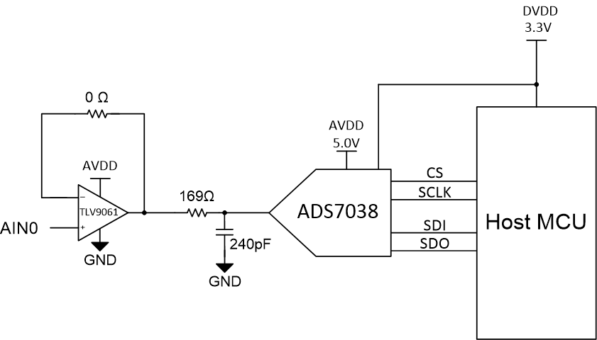
GUID-20201006-CA0I-5FCT-0HGL-KDPZQRHMW0GJ-low.gifFigure 4-1 Channel 0 Input Signal Buffer Circuit.