SNOSD57 June 2017 LF298-MIL
PRODUCTION DATA.
- 1 Features
- 2 Applications
- 3 Description
- 4 Revision History
- 5 Pin Configuration and Functions
- 6 Specifications
- 7 Parameter Measurement Information
- 8 Detailed Description
-
9 Application and Implementation
- 9.1 Application Information
- 9.2
Typical Applications
- 9.2.1 X1000 Sample and Hold
- 9.2.2 Sample and Difference Circuit
- 9.2.3 Ramp Generator With Variable Reset Level
- 9.2.4 Integrator With Programmable Reset Level
- 9.2.5 Output Holds at Average of Sampled Input
- 9.2.6 Increased Slew Current
- 9.2.7 Reset Stabilized Amplifier
- 9.2.8 Fast Acquisition, Low Droop Sample and Hold
- 9.2.9 Synchronous Correlator for Recovering Signals Below Noise Level
- 9.2.10 2-Channel Switch
- 9.2.11 DC and AC Zeroing
- 9.2.12 Staircase Generator
- 9.2.13 Differential Hold
- 9.2.14 Capacitor Hysteresis Compensation
- 10Power Supply Recommendations
- 11Layout
- 12Device and Documentation Support
- 13Mechanical, Packaging, and Orderable Information
1 Features
- Operates from ±5-V to ±18-V Supplies
- Less than 10-μs Acquisition Time
- Logic Input Compatible With TTL, PMOS, CMOS
- 0.5-mV Typical Hold Step at Ch = 0.01 µF
- Low Input Offset
- 0.002% Gain Accuracy
- Low Output Noise in Hold Mode
- Input Characteristics Do Not Change During Hold Mode
- High Supply Rejection Ratio in Sample or Hold
- Wide Bandwidth
- Space Qualified, JM38510
2 Applications
- Ramp Generators With Variable Reset Level
- Integrators With Programmable Reset Level
- Synchronous Correlators
- 2-Channel Switches
- DC and AC Zeroing
- Staircase Generators
3 Description
The LF298-MIL devices are monolithic sample-and-hold circuits that use BI-FET technology to obtain ultrahigh DC accuracy with fast acquisition of signal and low droop rate. Operating as a unity-gain follower, DC gain accuracy is 0.002% typical and acquisition time is as low as 6 µs to 0.01%. A bipolar input stage is used to achieve low offset voltage and wide bandwidth. Input offset adjust is accomplished with a single pin and does not degrade input offset drift. The wide bandwidth allows the LF298-MIL to be included inside the feedback loop of 1-MHz operational amplifiers without having stability problems. Input impedance of 1010 Ω allows high-source impedances to be used without degrading accuracy.
P-channel junction FETs are combined with bipolar devices in the output amplifier to give droop rates as low as 5 mV/min with a 1-µF hold capacitor. The JFETs have much lower noise than MOS devices used in previous designs and do not exhibit high temperature instabilities. The overall design ensures no feedthrough from input to output in the hold mode, even for input signals equal to the supply voltages.
Logic inputs on the LF298-MIL are fully differential with low input current, allowing for direct connection to TTL, PMOS, and CMOS. Differential threshold is
1.4 V. The LF298-MIL will operate from ±5-V to ±18-V supplies.
An A version is available with tightened electrical specifications.
Device Information(1)
| PART NUMBER | PACKAGE | BODY SIZE (NOM) |
|---|---|---|
| LF298-MIL | SOIC (14) | 8.65 mm × 3.91 mm |
| TO-99 (8) | 9.08 mm × 9.08 mm |
- For all available packages, see the orderable addendum at the end of the data sheet.
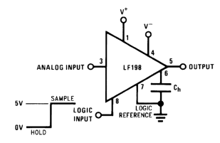
Typical Connection

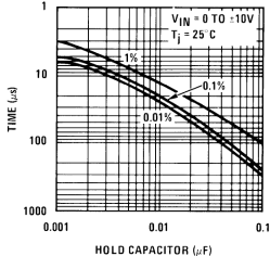
Acquisition Time
