ZHCSR78H July 2000 – November 2022 UCC28C40 , UCC28C41 , UCC28C42 , UCC28C43 , UCC28C44 , UCC28C45 , UCC38C40 , UCC38C41 , UCC38C42 , UCC38C43 , UCC38C44 , UCC38C45
PRODUCTION DATA
- 1 特性
- 2 应用
- 3 说明
- 4 Revision History
- 5 Device Comparison Table
- 6 Pin Configuration and Functions
- 7 Specifications
-
8 Detailed Description
- 8.1 Overview
- 8.2 Functional Block Diagram
- 8.3
Feature Description
- 8.3.1 Detailed Pin Description
- 8.3.2 Undervoltage Lockout
- 8.3.3 ±1% Internal Reference Voltage
- 8.3.4 Current Sense and Overcurrent Limit
- 8.3.5 Reduced-Discharge Current Variation
- 8.3.6 Oscillator Synchronization
- 8.3.7 Soft-Start Timing
- 8.3.8 Enable and Disable
- 8.3.9 Slope Compensation
- 8.3.10 Voltage Mode
- 8.4 Device Functional Modes
-
9 Application and Implementation
- 9.1 Application Information
- 9.2
Typical Application
- 9.2.1 Design Requirements
- 9.2.2
Detailed Design Procedure
- 9.2.2.1 Input Bulk Capacitor and Minimum Bulk Voltage
- 9.2.2.2 Transformer Turns Ratio and Maximum Duty Cycle
- 9.2.2.3 Transformer Inductance and Peak Currents
- 9.2.2.4 Output Capacitor
- 9.2.2.5 Current Sensing Network
- 9.2.2.6 Gate Drive Resistor
- 9.2.2.7 VREF Capacitor
- 9.2.2.8 RT/CT
- 9.2.2.9 Start-Up Circuit
- 9.2.2.10 Voltage Feedback Compensation
- 9.2.3 Application Curves
- 9.3 Power Supply Recommendations
- 9.4 Layout
- 10Device and Documentation Support
- 11Mechanical, Packaging, and Orderable Information
封装选项
请参考 PDF 数据表获取器件具体的封装图。
机械数据 (封装 | 引脚)
- D|8
- DGK|8
散热焊盘机械数据 (封装 | 引脚)
- DGK|8
订购信息
8.3.2 Undervoltage Lockout
Six sets of UVLO thresholds are available with turn-on and turnoff thresholds of: (14.5 V and 9 V), (8.4 V and 7.6 V), (7 V and 6.6 V) respectively. The first set is primarily intended for off-line and 48-V distributed power applications, where the wider hysteresis allows for lower frequency operation and longer soft-starting time of the converter. The second group of UVLO options is ideal for high frequency DC-DC converters typically running from a 12-VDC input. The third, and newest, set has been added to address battery powered and portable applications. Table 8-2 shows the maximum duty cycle and UVLO thresholds by device.
| MAXIMUM DUTY CYCLE (%) |
UVLO ON (V) |
UVLO OFF (V) |
DEVICE NUMBER |
|---|---|---|---|
| 100 | 14.5 | 9 | UCCx8C42 |
| 100 | 8.4 | 7.6 | UCCx8C43 |
| 100 | 7 | 6.6 | UCCx8C40 |
| 50 | 14.5 | 9 | UCCx8C44 |
| 50 | 8.4 | 7.6 | UCCx8C45 |
| 50 | 7 | 6.6 | UCCx8C41 |
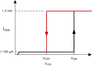
During UVLO the IC draws less than 100 µA of supply current. After crossing the turnon threshold, the device supply current increases to a maximum of 3 mA, typically 2.3 mA. This low start-up current allows the power supply designer to optimize the selection of the startup resistor value to provide a more efficient design. In applications where low component cost overrides maximum efficiency, the low run current of 2.3 mA (typical) allows the control device to run directly through the single resistor to (+) rail, rather than requiring a bootstrap winding on the power transformer, along with a rectifier. The start and run resistor for this case must also pass enough current to allow driving the primary switching MOSFET, which may be a few milliamps in small devices.
 Figure 8-2 UVLO ON and OFF
Profile