ZHCSR78H July 2000 – November 2022 UCC28C40 , UCC28C41 , UCC28C42 , UCC28C43 , UCC28C44 , UCC28C45 , UCC38C40 , UCC38C41 , UCC38C42 , UCC38C43 , UCC38C44 , UCC38C45
PRODUCTION DATA
- 1 特性
- 2 应用
- 3 说明
- 4 Revision History
- 5 Device Comparison Table
- 6 Pin Configuration and Functions
- 7 Specifications
-
8 Detailed Description
- 8.1 Overview
- 8.2 Functional Block Diagram
- 8.3
Feature Description
- 8.3.1 Detailed Pin Description
- 8.3.2 Undervoltage Lockout
- 8.3.3 ±1% Internal Reference Voltage
- 8.3.4 Current Sense and Overcurrent Limit
- 8.3.5 Reduced-Discharge Current Variation
- 8.3.6 Oscillator Synchronization
- 8.3.7 Soft-Start Timing
- 8.3.8 Enable and Disable
- 8.3.9 Slope Compensation
- 8.3.10 Voltage Mode
- 8.4 Device Functional Modes
-
9 Application and Implementation
- 9.1 Application Information
- 9.2
Typical Application
- 9.2.1 Design Requirements
- 9.2.2
Detailed Design Procedure
- 9.2.2.1 Input Bulk Capacitor and Minimum Bulk Voltage
- 9.2.2.2 Transformer Turns Ratio and Maximum Duty Cycle
- 9.2.2.3 Transformer Inductance and Peak Currents
- 9.2.2.4 Output Capacitor
- 9.2.2.5 Current Sensing Network
- 9.2.2.6 Gate Drive Resistor
- 9.2.2.7 VREF Capacitor
- 9.2.2.8 RT/CT
- 9.2.2.9 Start-Up Circuit
- 9.2.2.10 Voltage Feedback Compensation
- 9.2.3 Application Curves
- 9.3 Power Supply Recommendations
- 9.4 Layout
- 10Device and Documentation Support
- 11Mechanical, Packaging, and Orderable Information
封装选项
请参考 PDF 数据表获取器件具体的封装图。
机械数据 (封装 | 引脚)
- D|8
- DGK|8
散热焊盘机械数据 (封装 | 引脚)
- DGK|8
订购信息
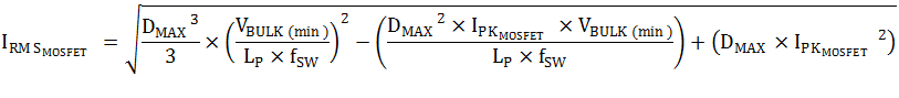
9.2.2.3 Transformer Inductance and Peak Currents
For this design example, the transformer magnetizing inductance is selected based upon the CCM condition. An inductance value that allows the converter to stay in CCM over a wider operating range before transitioning into discontinuous current mode is used to minimize losses due to otherwise high currents and also to decrease the output ripple. The design of the transformer in this example sizes the inductance so the converter enters CCM operation at approximately 10% load and minimum bulk voltage to minimize output ripple.
The inductor (LP) for a CCM flyback can be calculated using Equation 11.

where
- PIN is estimated by dividing the maximum output power (POUT) by the target efficiency (η)
- fSW is the switching frequency of the converter
For the UCC28C42 the switching frequency is equal to the oscillator frequency and is set to 110 kHz. Selecting fSW to be 110 kHz provides a good compromise between size of magnetics, switching losses, and places the first harmonic below the 150-kHz lower limit of EN55022. Therefore, the transformer inductance must be approximately 1.8 mH. A 1.5 mH inductance is chosen as the magnetizing inductance, LP, value for this design.
Based on calculated inductor value and the switching frequency, the current stress of the MOSFET and output diode can be calculated.
The peak current in the primary-side MOSFET of a CCM flyback can be calculated as shown in Equation 12.
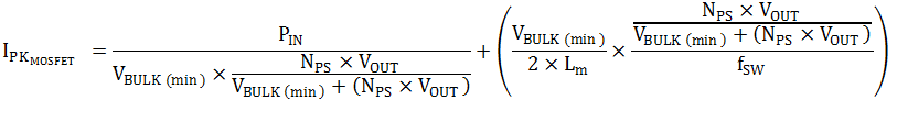
The MOSFET peak current is 1.36 A. The RMS current of the MOSFET is calculated to be 0.97 A as shown in Equation 13. Therefore, IRFB9N65A is selected to be used as the primary-side switch.
The output diode peak current is equal to the MOSFET peak current reflected to the secondary side.

The diode average current is equal to the total output current (4 A) combined with a required 60-V rating and 13.6-A peak current requirement, a 48CTQ060-1 is selected for the output diode.