ZHCSCP2 July 2014 UCC28880
PRODUCTION DATA.
- 1 特性
- 2 应用
- 3 说明
- 4 修订历史记录
- 5 Pin Configuration and Functions
- 6 Specifications
- 7 Detailed Description
-
8 Application and Implementation
- 8.1 Application Information
- 8.2
Typical Application
- 8.2.1 12-V, 100-mA Low-Side Buck Converter
- 8.2.2 12-V, 100-mA, High-Side Buck Converter
- 8.2.3
Additional UCC28880 Application Topologies
- 8.2.3.1 Low-Side Buck and LED Driver - Direct Feedback (level-shifted)
- 8.2.3.2 12-V, 100-mA High-Side Buck Converter
- 8.2.3.3 Non-Isolated, Low-Side Buck-Boost Converter
- 8.2.3.4 9.5 Non-Isolated, High-Side Buck-Boost Converter
- 8.2.3.5 9.6 Non-Isolated Flyback Converter
- 8.2.3.6 Isolated Flyback Converter
- 9 Power Supply Recommendations
- 10Layout
- 11器件和文档支持
- 12机械封装和可订购信息
7 Detailed Description
7.1 Overview
The UCC28880 integrates a controller and a 700-V power MOSFET into one monolithic device. The device also integrates a high-voltage current source, enabling start up and operation directly from the rectified mains voltage.
The low-quiescent current of the device enables excellent efficiency. The device is suitable for non-isolated AC-to-DC low-side buck and buck-boost configurations with level-shifted direct feedback, but also more traditional high-side buck, buck boost and low-power flyback converters with low standby power can be built using a minimum number of external components.
The device generates its own internal low-voltage supply (5 V referenced to the device’s ground, GND) from the integrated high-voltage current source. The PWM signal generation is based on a maximum constant ON-time, minimum OFF-time concept, with the triggering of the ON-pulse depending on the feedback voltage level. Each ON-pulse is followed by a minimum OFF-time to ensure that the power MOSFET is not continuously driven in an ON-state. The PWM signal is AND-gated with the signal from a current limit circuit. No internal clock is required, as the switching of the power MOSFET is load dependent. A special protection mechanism is included to avoid runaway of the inductor current when the converter operates with the output shorted or in other abnormal conditions that can lead to an uncontrolled increase of the inductor current. This special protection feature keeps the MOSFET current at a safe operating level. The device is also protected from other fault conditions with thermal shutdown, under-voltage lockout and soft-start features.
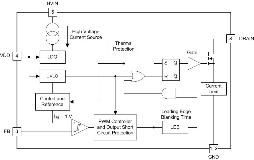
7.2 Functional Block Diagram
7.3 Feature Description
The device integrates a 700-V rated power MOSFET switch, a PWM controller, a high-voltage current source to supply a low-voltage power supply regulator, a bias and reference block, and the following protection features, current limiter, Over Temperature Protection (OTP), Under Voltage Lockout (UVLO) and overload protection for situations like short circuit at the output.
In low-side buck and buck-boost topologies, the external level-shifted direct feedback circuit can be implemented by two resistors and a high-voltage PNP transistor.
The positive high-voltage input of the converter node (VIN+) functions as a system reference ground for the output voltage in low-side topologies. In the low-side buck topology the output voltage is negative with respect to the positive high-voltage input (VIN+), and in low-side buck-boost topology the output voltage is positive with respect to the positive high-voltage input (VIN+).
In high-side buck configuration, as well as in non-isolated flyback configuration, the output voltage is positive with respect to the negative high-voltage input (VIN-), which is the system reference ground.
The device has a low-standby power consumption (no-load condition), only 18 mW (typical) when connected to a 230-VAC mains and 9 mW when connected to an 115-VAC mains.
The standby power does not include the power dissipated in the external feedback path, the power dissipated in the external pre-load, the inductor in the freewheeling diode and the converter input stage (rectifiers and filter).
7.4 Device Functional Modes
7.4.1 Startup Operation
The device includes a high-voltage current source connected between the HVIN pin and the internal supply for the regulator. When the voltage on the HVIN pin rises, the current source is activated and starts to supply current to the internal 5-V regulator. The 5-V regulator charges the external capacitor connected between VDD pin and GND pin. When the VDD voltage exceeds the VDD turn on threshold (VVDD(on)) device starts operations. The minimum voltage across HVIN and GND pins to ensure enough current to charge the capacitance on VDD pin is VHVIN(min). At the First switching cycle the minimum MOSFET off time is set to be > 100 μs and cycle-by-cycle is progressively reduced up to tOFF(min) providing soft start.
7.4.2 Feedback and Voltage Control Loop
The feedback circuit consists of a voltage comparator with the positive input connected to an internal reference voltage (referenced to GND) and the negative input connected to FB pin. When the feedback voltage at the FB pin is below the reference voltage VFB_TH logic high is generated at the comparator output. This logic high triggers the PWM controller, which generates the PWM signal turning on the MOSFET. When the feedback voltage at the FB pin is above the reference voltage, it indicates that the output voltage of the converter is above the targeted output voltage set by the external feedback circuitry and MOSFET cannot be turned on.
7.4.3 PWM Controller
The PWM controller's input comes from the feedback comparator. When the feedback comparator output goes high, the PWM controller is triggered. This starts the ON-time generation. The ON-time pulse is defined as tON(max) and at the end of every ON-time pulse an OFF-time (logic low) pulse starts. The OFF-time pulse is long as tOFF(min) during converter normal operation, it can be longer up to tOFF(ovl) at start up or if risk of inductor current runaway is detected. The output of the PWM controller is the PWM signal (See Figure 11). After the OFF-time pulse has ended, the PWM controller can again receive the feedback comparator’s output. If the feedback comparator’s output is still high, then a new ON-time pulse followed by an OFF-time pulse is generated for the PWM signal. If the feedback comparator’s output is low at the point the OFF-time has ended, then the PWM controller continues to output a logic low signal at the output (the PWM signal). The PWM signal stays low until the feedback comparator output goes high, at which point the PWM controller is again triggered, and the ON-time + OFF-time pulse is generated.
The PWM controller does not need a clock signal, and the PWM signal is load dependent. The PWM signal’s maximum frequency is set to fSW(max) = (1/(tON(max) + tOFF(min))) which occurs when the voltage on the FB pin is continuously below VFB_TH.
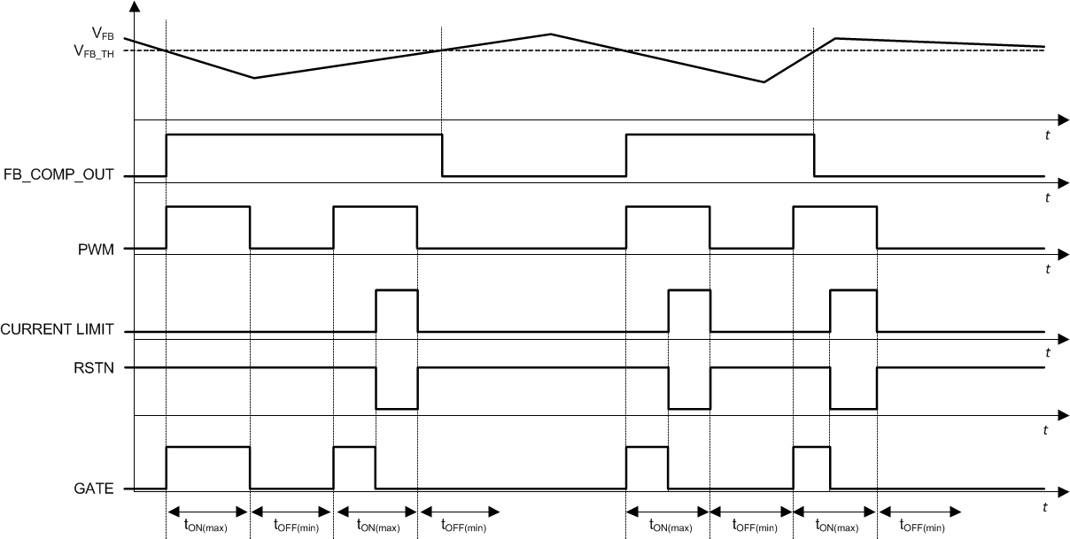 Figure 11. UCC28880 Timing Diagram
7.4.4 Current Limit
The current limit circuit senses the current through the power MOSFET. The sensing circuit is located between the source of the power MOSFET and the GND pin. When the current in the power MOSFET exceeds the threshold ILIMIT, the internal current limit signal goes high, which sets the internal RSTN signal low. This disables the power MOSFET by driving its gate low. The current limit signal is set back low after the falling edge of the PWM signal. After the rising edge of the GATE signal, there is a blanking time. During this blanking time, the current limit signal cannot go high.
7.4.5 Inductor Current Runaway Protection
To protect the device from overload conditions, including a short circuit at the output, the PWM controller incorporates a protection feature which prevents the inductor current from runaway. When the output is shorted the inductor demagnetization is very slow, low di/dt, and when the next switching cycle starts energy stored in the inductance is still high. After the MOSFET switches on, the current starts to rise from pre-existing DC value and reaches the current-limit value in a short duration of time. Because of the intrinsic minimum on-time of the device the MOSFET on-time cannot be lower than tMIN, in an overload or output short circuit the energy inductance is not discharged sufficiently during MOSFET off-time, it is possible to lose control of the current leading to a runaway of the inductor current. To avoid this, if the ON time is less than tON_TO (tON_TO is a device internal time out), the controller increases the MOSFET OFF time (tOFF). If the MOSFET ON-time is longer than tON_OL then tOFF is decreased. The controller increases tOFF, cycle-by-cycle, through discrete steps until the ON-time continues to stay below tON_TO. The tOFF is increased up to tOFF(ovl) after that, if teh ON-time is still below tON_OL the off time is kept equal to tOFF(ovl). The controller decreases tOFF cycle-by-cycle until the ON-time continues to stay above tON_TO up to tOFF(min). This mechanism prevents control loss of the inductor current and prevents over stress of the MOSFET (see typical waveforms in Figure 12 and Figure 13). At start up, the tOFF is set to tOFF(ovl) and reduced cycle-by-cycle (if the ON time is longer than tON_TO) up to tOFF(min) providing a soft start for the power stage.
 Figure 12. Current Runaway Protection Logic Timing Diagram
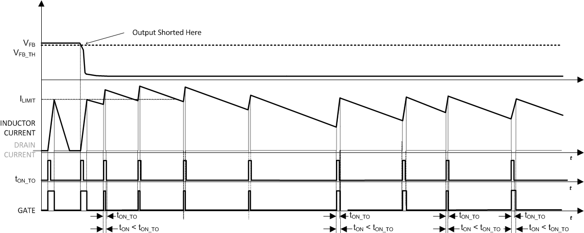 Figure 13. Current Runaway Protection, Inductor and MOSFET Current
A minimal value needs to be imposed on the inductance value to avoid nuisance tripping of the protection feature that prevents the loss of control of the inductor current. Inadvertent operation of the protection feature limits the output-power capability of the converter. This condition depends on the converter's maximum input operating voltage and temperature. Use Equation 1 to calculate your minimum inductance value.
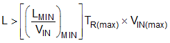
The value of Equation 1 can be found by characterization graph of Figure 10.
If the inductance value is too low, such that the MOSFET on-time is always less than tON_TO timeout and the device progressively increases the MOSFET off-time up to tOFF(ovl), the output power is reduced and the converter fails to supply the load.
7.4.6 Over-Temperature Protection
If the junction temperature rises above TJ(stop), the over-temperature protection is triggered. This disables the power MOSFET switching. To re-enable the switching of the MOSFET the junction temperature has to fall by TJ(hyst) below the TJ(stop) where the device moves out of over temperature.