ZHCSCP2 July   2014 UCC28880

PRODUCTION DATA.  

  1. 特性
  2. 应用
  3. 说明
  4. 修订历史记录
  5. Pin Configuration and Functions
  6. Specifications
    1. 6.1 Absolute Maximum Ratings
    2. 6.2 Handling Ratings
    3. 6.3 Recommended Operating Conditions
    4. 6.4 Thermal Information
    5. 6.5 Electrical Characteristics
    6. 6.6 Switching Characteristics
    7. 6.7 Typical Characteristics
  7. Detailed Description
    1. 7.1 Overview
    2. 7.2 Functional Block Diagram
    3. 7.3 Feature Description
    4. 7.4 Device Functional Modes
      1. 7.4.1 Startup Operation
      2. 7.4.2 Feedback and Voltage Control Loop
      3. 7.4.3 PWM Controller
      4. 7.4.4 Current Limit
      5. 7.4.5 Inductor Current Runaway Protection
      6. 7.4.6 Over-Temperature Protection
  8. Application and Implementation
    1. 8.1 Application Information
    2. 8.2 Typical Application
      1. 8.2.1 12-V, 100-mA Low-Side Buck Converter
        1. 8.2.1.1 Design Requirements
        2. 8.2.1.2 Detailed Design Procedure
          1. 8.2.1.2.1 Input Stage (RF, D2, D3, C1, C2, L2)
          2. 8.2.1.2.2 Regulator Capacitor (CVDD)
          3. 8.2.1.2.3 Freewheeling Diode (D1)
          4. 8.2.1.2.4 Inductor (L1)
          5. 8.2.1.2.5 Output Capacitor (CL)
          6. 8.2.1.2.6 Load Resistor (RL)
          7. 8.2.1.2.7 Feedback Path (Q1, RFB1, RFB2)
        3. 8.2.1.3 Application Curves
      2. 8.2.2 12-V, 100-mA, High-Side Buck Converter
        1. 8.2.2.1 Design Requirements
        2. 8.2.2.2 Detailed Design Procedure
          1. 8.2.2.2.1 Feedback path (CFB, RFB1 and RFB2) and Load Resistor (RL)
        3. 8.2.2.3 Application Curves
      3. 8.2.3 Additional UCC28880 Application Topologies
        1. 8.2.3.1 Low-Side Buck and LED Driver - Direct Feedback (level-shifted)
        2. 8.2.3.2 12-V, 100-mA High-Side Buck Converter
        3. 8.2.3.3 Non-Isolated, Low-Side Buck-Boost Converter
        4. 8.2.3.4 9.5 Non-Isolated, High-Side Buck-Boost Converter
        5. 8.2.3.5 9.6 Non-Isolated Flyback Converter
        6. 8.2.3.6 Isolated Flyback Converter
  9. Power Supply Recommendations
  10. 10Layout
    1. 10.1 Layout Guidelines
    2. 10.2 Layout Example
  11. 11器件和文档支持
    1. 11.1 Trademarks
    2. 11.2 Electrostatic Discharge Caution
    3. 11.3 术语表
  12. 12机械封装和可订购信息

封装选项

机械数据 (封装 | 引脚)
散热焊盘机械数据 (封装 | 引脚)
订购信息

10 Layout

10.1 Layout Guidelines

  • In both buck and buck-boost low-side configurations, the copper area of the switching node DRAIN should be minimized to reduce EMI.
  • Similarly, the copper area of the FB pin should be minimized to reduce coupling to feedback path. Loop CL, Q1, RFB1 should be minimized to reduce coupling to feedback path.
  • In buck and buck-boost high side the GND, VDD and FB pins are all part of the switching node so the copper area connected with these pins should be minimized
  • Minimum distance between 700-V coated traces is 1.41 mm (60 mils).

10.2 Layout Example

Figure 27 shows and example PCB layout for UCC28880 in low-side buck configuration.

layoutexample2_lusc05.gif
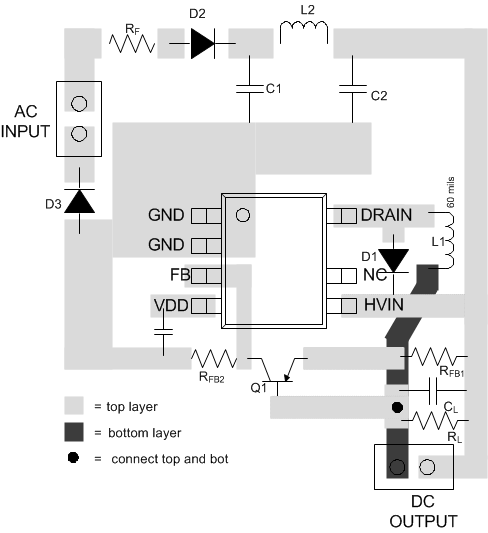
Figure 27. UCC28880 Layout Example