ZHCSBD7B August 2013 – October 2014 UCC27524A
PRODUCTION DATA.
- 1 特性
- 2 应用
- 3 说明
- 4 修订历史记录
- 5 说明(继续)
- 6 Pin Configuration and Functions
- 7 Specifications
- 8 Detailed Description
- 9 Applications and Implementation
- 10Power Supply Recommendations
- 11Layout
- 12器件和文档支持
- 13机械封装和可订购信息
封装选项
机械数据 (封装 | 引脚)
散热焊盘机械数据 (封装 | 引脚)
- DGN|8
订购信息
6 Pin Configuration and Functions
8-Pin
D, DGN Package
Top View
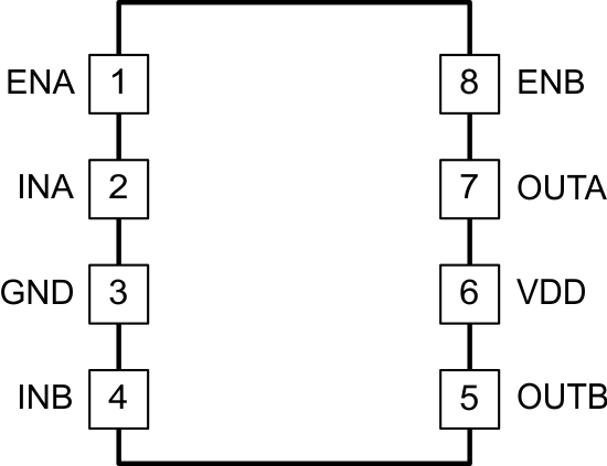
Pin Functions
| PIN | I/O | DESCRIPTION | |
|---|---|---|---|
| NAME | NO. | ||
| ENA | 1 | I | Enable input for Channel A: ENA is biased LOW to disable the Channel A output regardless of the INA state. ENA is biased HIGH or left floating to enable the Channel A output. ENA is allowed to float; hence the pin-to-pin compatibility with the UCC2732X N/C pin. |
| ENB | 8 | I | Enable input for Channel B: ENB is biased LOW to disables the Channel B output regardless of the INB state. ENB is biased HIGH or left floating to enable Channel B output. ENB is allowed to float hence; the pin-to-pin compatibility with the UCC2752A N/C pin. |
| GND | 3 | - | Ground: All signals are referenced to this pin. |
| INA | 2 | I | Input to Channel A: INA is the non-inverting input in the UCC27524A device. OUTA is held LOW if INA is unbiased or floating. |
| INB | 4 | I | Input to Channel B: INB is the non-inverting input in the UCC27524A device. OUTB is held LOW if INB is unbiased or floating. |
| OUTA | 7 | O | Output of Channel A |
| OUTB | 5 | O | Output of Channel B |
| VDD | 6 | I | Bias supply input |