SLUS704C FEBRUARY 2007 – December 2014 UCC27423-EP , UCC27424-EP
PRODUCTION DATA.
10 Layout
10.1 Layout Guidelines
Circuit layout is extremely critical in gate drive circuit. As shows in graphics below there might be considerable distance between the PWM controller and the MOSFET. This distance introduces parasitics inductance due to the loop formed by the gate drive and ground return trace, which can slow down the switching speed and can cause ringing at the gate drive waveform. To reduce the inductance linked to the gate drive connection, a wider PCB trace is desirable. Gate driver incorporates short propagation delays and powerful output stage capable of delivering large current peaks with fast rise and fall times at the gate of the power switch to facilitate voltage transition very quickly. Very high peak current result in high di/dt which can cause unacceptable ringing if the trace lengths and impedances are not well controlled.
- Locate the device driver as close as possible to power device in order to minimize the length of high-current traces between the output pins and the gate of the power device.
- Locate the VDD bypass capacitors between VDD and GND as close as possible to the driver with minimal trace length to improve the noise filtering. These capacitors support high-peak current being drawn from VDD during turnon of power MOSFET. The use of low inductance SMD components such as chip resistors and chip capacitors is highly recommended.
- The turn-on and turn-off current loop paths (driver device, power MOSFET and VDD bypass capacitor) should be minimized as much as possible in order to keep the stray inductance to a minimum. High di/dt is established in these loops at two instances - during turn-on and turn-off transients, which will induce significant voltage transients on the output pin of the driver device and gate of the power switch.
- Wherever possible parallel the source and return traces, such as output and input signals.
- Star-point grounding is a good way to minimize noise coupling from one current loop to another. The GND of the driver should be connected to the other circuit nodes such as source of power switch and ground of PWM controller at one point. The connected paths should be as short as possible to reduce inductance and be as wide as possible to reduce resistance.
- Use a ground plane to provide noise shielding. Fast rise and fall times at OUT may corrupt the input signals during transition. The ground plane must not be a conduction path for any current loop. Instead the ground plane must be connected to the star-point with one single trace to establish the ground potential. In addition to noise shielding, the ground plane can help in power dissipation as well.
10.2 Layout Example
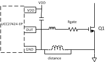 Figure 29. Noise Shielding Example Layout
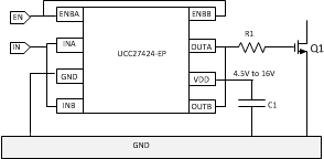 Figure 30. PCB Layout Example
10.3 Thermal Considerations
The useful range of a driver is greatly affected by the drive power requirements of the load and the thermal characteristics of the IC package. For a power driver to be useful over a particular temperature range, the package must allow for the efficient removal of the heat produced, while keeping the junction temperature within rated limits.
As shown in Power Dissipation Ratings, the SOIC-8 (D) package has a power rating of around 0.5 W with TA = 70°C. This limit is imposed in conjunction with the power derating factor also given in the table. Note that the power dissipation in the earlier example is 0.432 W with a 10-nF load, 12 VDD, switched at 300 kHz. Thus, only one load of this size could be driven using the D package, even if the two onboard drivers are paralleled. The difficulties with heat removal limit the drive available in the older packages.
The MSOP-8 PowerPAD (DGN) package significantly relieves this concern by offering an effective means of removing the heat from the semiconductor junction. As shown in reference (3), the PowerPAD packages offer a leadframe die pad that is exposed at the base of the package. This pad is soldered to the copper on the PCB directly underneath the IC package, reducing the RθJC to 4.7°C/W. Data is presented in reference (3) to show that the power dissipation can be quadrupled in the PowerPAD package configuration when compared to the standard packages. The PCB must be designed with thermal lands and thermal vias to complete the heat-removal subsystem, as summarized in reference (4). This allows a significant improvement in heatsinking over that available in the D package and is shown to more than double the power capability of the D package. Note that the PowerPAD package is not directly connected to any leads of the package. However, it is electrically and thermally connected to the substrate, which is the ground of the device.