ZHCSIF6D March 2008 – November 2023 UCC27324-Q1
PRODUCTION DATA
- 1
- 1 特性
- 2 应用
- 3 说明
- 4 Pin Configuration and Functions
-
5 Specifications
- 5.1 Absolute Maximum Ratings
- 5.2 ESD Ratings
- 5.3 Recommended Operating Conditions
- 5.4 Thermal Information
- 5.5 Overall Electrical Characteristics
- 5.6 Power Dissipation Characteristics
- 5.7 Input (INA, INB) Electrical Characteristics
- 5.8 Output (OUTA, OUTB) Electrical Characteristics
- 5.9 Switching Characteristics
- 5.10 Typical Characteristics
- 6 Detailed Description
- 7 Application and Implementation
- 8 Power Supply Recommendations
- 9 Layout
- 10Device and Documentation Support
- 11Revision History
- 12Mechanical, Packaging, and Orderable Information
7.2.2.2 Source and Sink Capabilities During Miller Plateau
Large power MOSFETs present a large load to the control circuitry. Proper drive is required for efficient, reliable operation. The UCC27324-Q1 drivers have been optimized to provide maximum drive to a power MOSFET during the Miller plateau region of the switching transition. This interval occurs while the drain voltage is swinging between the voltage levels dictated by the power topology, requiring the charging or discharging of the drain-gate capacitance with current supplied or removed by the driver.
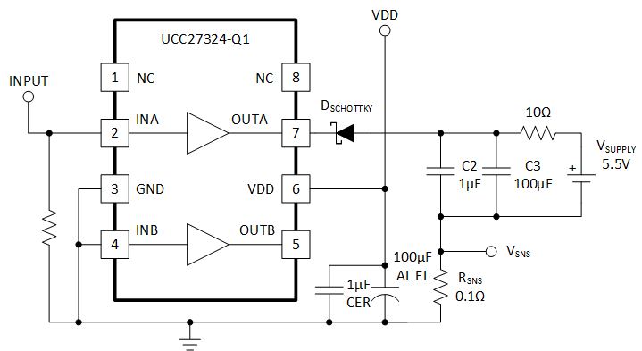
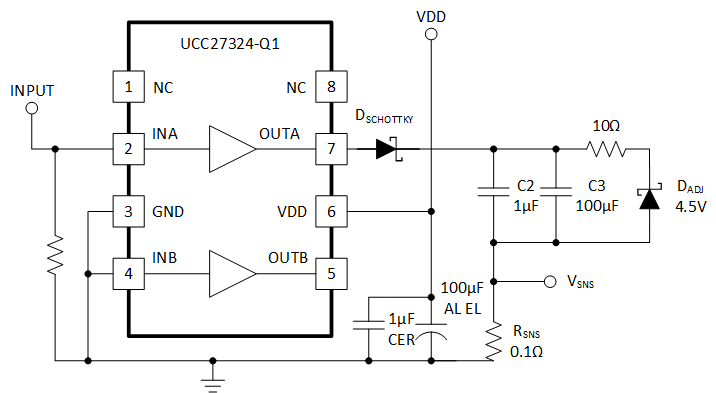
Two circuits are used to test the current capabilities of the UCC27324-Q1 driver. In each case, external circuitry is added to clamp the output near 5 V while the device is sinking or sourcing current. An input pulse of 250 ns is applied at a frequency of 1 kHz in the proper polarity for the respective test. In each test, there is a transient period when the current peaked up and then settled down to a steady-state value. The noted current measurements are made at a time of 200 ns after the input pulse is applied, after the initial transient.
The circuit in Figure 7-3 is used to verify the current sink capability when the output of the driver is clamped at approximately 5 V, a typical value of gate-source voltage during the Miller plateau region. The UCC27324-Q1 is found to sink 4.5 A at VDD = 15 V and 4.28 A at VDD = 12 V.
 Figure 7-3 Current Sink Test Circuit
The circuit in Figure 7-4 is used to test the current source capability with the output clamped to approximately 5 V with a string of Zener diodes. The UCC27324-Q1 device can source 4.8 A at VDD = 15 V and 3.7 A at VDD = 12 V.
 Figure 7-4 Current Source Test Circuit
The current-sink capability is slightly stronger than the current source capability at lower VDD because of the differences in the structure of the bipolar-MOSFET power output section, where the current source is a P-channel MOSFET and the current sink has an N-channel MOSFET.
In a large majority of applications, the fact that the turn-off capability of a driver is stronger than the turn-on capability is advantageous which helps to ensure that the MOSFET is held off during common power-supply transients that may turn the device back on.