ZHCSJY8E june 2019 – february 2021 UCC256402 , UCC256403 , UCC256404
PRODUCTION DATA
- 1 特性
- 2 应用
- 3 说明
- 4 Revision History
- 5 Pin Configuration and Functions
- 6 Specifications
-
7 Detailed Description
- 7.1 Overview
- 7.2 Functional Block Diagram
- 7.3 Feature Description
- 7.4
Device Functional Modes
- 7.4.1 High Voltage Start-Up
- 7.4.2 X-Capacitor Discharge
- 7.4.3 Burst Mode Control
- 7.4.4
System State Machine
-
Application and Implementation
- 8.1 Application Information
- 8.2
Typical Application
- 8.2.1 Design Requirements
- 8.2.2
Detailed Design Procedure
- 8.2.2.1 LLC Power Stage Requirements
- 8.2.2.2 LLC Gain Range
- 8.2.2.3 Select Ln and Qe
- 8.2.2.4 Determine Equivalent Load Resistance
- 8.2.2.5 Determine Component Parameters for LLC Resonant Circuit
- 8.2.2.6 LLC Primary-Side Currents
- 8.2.2.7 LLC Secondary-Side Currents
- 8.2.2.8 LLC Transformer
- 8.2.2.9 LLC Resonant Inductor
- 8.2.2.10 LLC Resonant Capacitor
- 8.2.2.11 LLC Primary-Side MOSFETs
- 8.2.2.12 LLC Rectifier Diodes
- 8.2.2.13 LLC Output Capacitors
- 8.2.2.14 HV Pin Series Resistors
- 8.2.2.15 BLK Pin Voltage Divider
- 8.2.2.16 ISNS Pin Differentiator
- 8.2.2.17 VCR Pin Capacitor Divider
- 8.2.2.18 BW Pin Voltage Divider
- 8.2.2.19 Soft Start and Burst Mode Programming
- 8.2.3 Application Curves
-
Application and Implementation
- 8 Power Supply Recommendations
- 9 Layout
- 10Device and Documentation Support
7.3.8 High Voltage Gate Driver
LO is the low-side gate driver output. The gate driver is supplied by the 13-V RVCC rail.
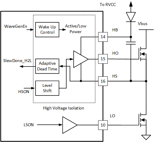
The high-side driver module consists of three physical device pins. HB and HS form the positive and negative bias rail, respectively, of the high-side driver, and HO connects to the gate of the upper half-bridge MOSFET.
During periods when the lower half-bridge MOSFET is conducting, HS is shorted to GND via the conducting lower MOSFET. At this time power for the high-side driver is obtained from RVCC via the high voltage diode DBOOT, and capacitor CBOOT is charged to RVCC minus the forward drop on the diode.
During periods when the upper half-bridge MOSFET is conducting, HS is connected to the LLC input voltage rail. At this time the HV diode is reverse biased and the high-side driver is powered by the charge stored in CBOOT.
Both the high-side and low-side gate drivers have under voltage lock out (UVLO) protection. The low-side gate driver UVLO is implemented on RVCC; the high-side gate driver UVLO is implemented on (HB - HS) voltage.
When operating at light load, UCC25640x enters burst mode. During the burst off period, the gate driver enters low power mode to reduce power consumption.
The block diagram of the gate driver is shown in Figure 7-10.
 Figure 7-10 Gate Driver Block Diagram