ZHCSJY8E june   2019  – february 2021 UCC256402 , UCC256403 , UCC256404

PRODUCTION DATA  

  1. 特性
  2. 应用
  3. 说明
  4. Revision History
    1.     Device Comparison Table
  5. Pin Configuration and Functions
    1.     Pin Functions
  6. Specifications
    1. 6.1 Absolute Maximum Ratings
    2. 6.2 ESD Ratings
    3. 6.3 Recommended Operating Conditions
    4. 6.4 Thermal Information
    5. 6.5 Electrical Characteristics
    6. 6.6 Switching Characteristics
    7. 6.7 Typical Characteristics
  7. Detailed Description
    1. 7.1 Overview
    2. 7.2 Functional Block Diagram
    3. 7.3 Feature Description
      1. 7.3.1 Hybrid Hysteretic Control
      2. 7.3.2 Regulated 13-V Supply
      3. 7.3.3 Feedback Chain
        1. 7.3.3.1 Optocoupler Feedback Signal Input and Bias
        2. 7.3.3.2 FB Pin Voltage Clamp
        3. 7.3.3.3 "Pick Lower Value" Block and Soft Start Multiplexer
        4. 7.3.3.4 Pick Higher Block and Burst Mode Multiplexer
        5. 7.3.3.5 VCR Comparators
      4. 7.3.4 Resonant Capacitor Voltage Sensing
      5. 7.3.5 Resonant Current Sensing
      6. 7.3.6 Bulk Voltage Sensing
      7. 7.3.7 Output Voltage Sensing
      8. 7.3.8 High Voltage Gate Driver
        1. 7.3.8.1 Adaptive Dead Time Control
      9. 7.3.9 Protections
        1. 7.3.9.1 ZCS Region Prevention
        2. 7.3.9.2 Over Current Protection (OCP)
        3. 7.3.9.3 Bias Winding Over Voltage Protection (BWOVP)
        4. 7.3.9.4 Input Under Voltage Protection (VINUVP)
        5. 7.3.9.5 Input Over Voltage Protection (VINOVP)
        6. 7.3.9.6 Boot UVLO
        7. 7.3.9.7 RVCC UVLO
        8. 7.3.9.8 Over Temperature Protection (OTP)
    4. 7.4 Device Functional Modes
      1. 7.4.1 High Voltage Start-Up
      2. 7.4.2 X-Capacitor Discharge
      3. 7.4.3 Burst Mode Control
        1. 7.4.3.1 Soft-Start and Burst-Mode Threshold
        2. 7.4.3.2 BMTL/BMTH Ratio Programming
      4. 7.4.4 System State Machine
        1.       Application and Implementation
          1. 8.1 Application Information
          2. 8.2 Typical Application
            1. 8.2.1 Design Requirements
            2. 8.2.2 Detailed Design Procedure
              1. 8.2.2.1  LLC Power Stage Requirements
              2. 8.2.2.2  LLC Gain Range
              3. 8.2.2.3  Select Ln and Qe
              4. 8.2.2.4  Determine Equivalent Load Resistance
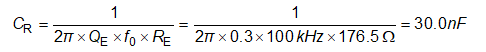
              5. 8.2.2.5  Determine Component Parameters for LLC Resonant Circuit
              6. 8.2.2.6  LLC Primary-Side Currents
              7. 8.2.2.7  LLC Secondary-Side Currents
              8. 8.2.2.8  LLC Transformer
              9. 8.2.2.9  LLC Resonant Inductor
              10. 8.2.2.10 LLC Resonant Capacitor
              11. 8.2.2.11 LLC Primary-Side MOSFETs
              12. 8.2.2.12 LLC Rectifier Diodes
              13. 8.2.2.13 LLC Output Capacitors
              14. 8.2.2.14 HV Pin Series Resistors
              15. 8.2.2.15 BLK Pin Voltage Divider
              16. 8.2.2.16 ISNS Pin Differentiator
              17. 8.2.2.17 VCR Pin Capacitor Divider
              18. 8.2.2.18 BW Pin Voltage Divider
              19. 8.2.2.19 Soft Start and Burst Mode Programming
            3. 8.2.3 Application Curves
  8. Power Supply Recommendations
    1. 8.1 VCC Pin Capacitor
    2. 8.2 Boot Capacitor
    3. 8.3 RVCC Pin Capacitor
  9. Layout
    1. 9.1 Layout Guidelines
    2. 9.2 Layout Example
  10. 10Device and Documentation Support
    1. 10.1 Documentation Support
      1. 10.1.1 Related Documentation
    2. 10.2 Related Links
    3. 10.3 Receiving Notification of Documentation Updates
    4. 10.4 Community Resources
    5. 10.5 Trademarks
      1.      Mechanical, Packaging, and Orderable Information

封装选项

机械数据 (封装 | 引脚)
散热焊盘机械数据 (封装 | 引脚)
订购信息

Determine Component Parameters for LLC Resonant Circuit

Before determining the resonant tank component parameters, a nominal switching frequency (resonant frequency) should be selected. In this design, 100 kHz is selected as the resonant frequency.

Equation 12. GUID-25C6E322-6515-4A47-99BC-ECF21C59B3B4-low.gif

The resonant tank parameters can be calculated as the following:

Equation 13. GUID-0BCB4674-A735-4D6E-9C7E-3A3BD4BCF03C-low.gif
Equation 14. GUID-6B8B0682-05AD-447E-988B-9CFD24D0E632-low.gif
Equation 15. GUID-26810A8A-5197-4B06-8015-7C2B646DFD27-low.gif

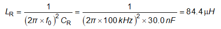
After the preliminary parameters are selected, find the closest actual component value that is available, re-check the gain curve with the selected parameters, and then run time domain simulation to verify the circuit operation.

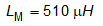
The following resonant tank parameters are:

Equation 16. GUID-29320665-85AE-4E42-A557-EB3F9F0B3068-low.gif
Equation 17. GUID-57502126-6261-46C6-9FAA-7F11DC13E934-low.gif
Equation 18. GUID-84BB018A-CA5C-493A-8874-AF9261282755-low.gif

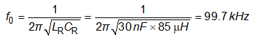
Based on the final resonant tank parameters, the resonant frequency can be calculated:

Equation 19. GUID-56BCCA73-A039-4CED-9F9E-16311E75150C-low.gif

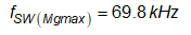
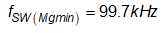
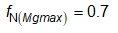
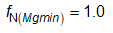
Based on the new LLC gain curve, the normalized switching frequency at maximum and minimum gain are given by:

Equation 20. GUID-88711127-B066-49E0-84DB-A0CBBA850702-low.gif
Equation 21. GUID-190B53B6-1B41-4C72-B585-2507ADAA7E7C-low.gif

The maximum and minimum switching frequencies are:

Equation 22. GUID-B31F7470-B2D7-4A8B-B6E2-4883D0E7D47F-low.gif
Equation 23. GUID-1B0F8D70-3749-42BB-902E-7DCCDBCBAD68-low.gif