ZHCSFA8 May 2016 TUSB501-Q1
PRODUCTION DATA.
9 Detailed Description
9.1 Overview
When 5 Gbps SuperSpeed USB signals travel across a PCB or cable, signal integrity degrades due to loss and inter-symbol interference. The TUSB501-Q1 recovers incoming data by applying equalization that compensates for channel loss, and drives out signals with a high differential voltage. This extends the possible channel length, and enables systems to pass USB 3.0 compliance.
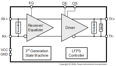
The TUSB501-Q1 advanced state machine makes it transparent to hosts and devices. After power up, the TUSB501-Q1 periodically performs receiver detection on the TX pair. If it detects a SuperSpeed USB receiver, the RX termination is enabled, and the TUSB501-Q1 is ready to re-drive.
The device aggressive Low-Power Architecture operates at a 3.3-V power supply and achieves enhanced performance, as lower as 3 mW with no connection and 126 mW in active state. The receiver equalizer has three gain settings that are controlled by terminal EQ: 3 dB, 6 dB, and 9 dB. The equalization should be set based on amount of insertion loss in the channel before the TUSB501-Q1. Likewise, the output driver supports configuration of De-Emphasis and Output Swing (terminals DE and OS). The automatic LFPS De-Emphasis control further enables the system to be USB3.0 compliant. The TUSB501-Q1 operates over the industrial temperature range of -40ºC to 85ºC in a small 2 x 2 mm WSON package.
Table 1. Control Pin Effects (Typical Values)
| PIN | DESCRIPTION | LOGIC STATE | GAIN |
|---|---|---|---|
| EQ | Equalization Amount | Low | 3 dB |
| Floating | 6 dB | ||
| High | 9 dB |
| PIN | DESCRIPTION | LOGIC STATE | OUTPUT DIFFERENTIAL VOLTAGE FOR THE TRANSITION BIT |
|---|---|---|---|
| OS | Output Swing Amplitude | Low | 930 mVpp |
| High | 1300 mVpp |
| PIN | DESCRIPTION | LOGIC STATE | DE-EMPHASIS RATIO (1) | |
|---|---|---|---|---|
| FOR OS = LOW | FOR OS = HIGH | |||
| DE | De-Emphasis Amount | Low | 0 dB | –2.6 dB |
| Floating | –3.5 dB | –5.9 dB | ||
| High | –6.2 dB | –8.3 dB | ||
9.2 Functional Block Diagram

9.3 Feature Description
9.3.1 Receiver Equalization
The purpose of receiver equalization is to compensate for channel insertion loss and inter-symbol interference in the system before the input of the TUSB501-Q1. The receiver overcomes these losses by attenuating the low frequency components of the signals with respect to the high frequency components. The proper gain setting should be selected to match the channel insertion loss before the input of the TUSB501-Q1.
9.3.2 De-Emphasis Control and Output Swing
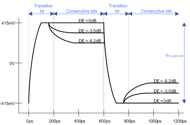
The differential driver output provides selectable de-emphasis and output swing control in order to achieve USB3.0 compliance. The TUSB501-Q1 offers a unique way to adjust output de-emphasis and transmitter swing based on the OS and DE terminals. The level of de-emphasis required in the system depends on the channel length after the output of the re-driver.
 Figure 7. Transmitter Differential Voltage, OS = L
9.3.3 Automatic LFPS Detection
The TUSB501-Q1 features an intelligent low frequency periodic signaling (LFPS) controller. The controller senses the low frequency signals and automatically disables the driver de-emphasis, for full USB3.0 compliance.
9.3.4 Automatic Power Management
The TUSB501-Q1 deploys RX detect, LFPS signal detection and signal monitoring to implement an automatic power management scheme to provide active, U2/U3 and disconnect modes. The automatic power management is driven by an advanced state machine, which is implemented to manage the device such that the re-driver operates smoothly in the links.
9.4 Device Functional Modes
9.4.1 Disconnect Mode
The Disconnect mode is the lowest power state of the TUSB501-Q1. In this state, the TUSB501-Q1 periodically checks for far-end receiver termination on both TX. Upon detection of the far-end receiver’s termination on both ports, the TUSB501-Q1 will transition to U0 mode.
9.4.2 U Modes
9.4.2.1 U0 Mode
The U0 mode is the highest power state of the TUSB501-Q1. Anytime super-speed traffic is being received, theTUSB501-Q1 remains in this mode.
9.4.2.2 U2/U3 Mode
Next to the disconnect mode, the U2/U3 mode is next lowest power state. While in this mode, the TUSB501-Q1 periodically performs far-end receiver detection.