ZHCSGH5D August   2017  – May 2019 TUSB1042I

PRODUCTION DATA.  

  1. 特性
  2. 应用
  3. 说明
    1.     Device Images
      1.      简化电路原理图
      2.      TUSB1042I 眼图
  4. 修订历史记录
  5. Pin Configuration and Functions
    1.     Pin Functions
  6. Specifications
    1. 6.1  Absolute Maximum Ratings
    2. 6.2  ESD Ratings
    3. 6.3  Recommended Operating Conditions
    4. 6.4  Thermal Information
    5. 6.5  Power Supply Characteristics
    6. 6.6  DC Electrical Characteristics
    7. 6.7  AC Electrical Characteristics
    8. 6.8  DCI Specific Electrical Characteristics
    9. 6.9  Timing Requirements
    10. 6.10 Switching Characteristics
    11. 6.11 Typical Characteristics
  7. Parameter Measurement Information
  8. Detailed Description
    1. 8.1 Overview
    2. 8.2 Functional Block Diagram
    3. 8.3 Feature Description
      1. 8.3.1 USB 3.1
      2. 8.3.2 4-level Inputs
      3. 8.3.3 Receiver Linear Equalization
    4. 8.4 Device Functional Modes
      1. 8.4.1 Device Configuration in GPIO Mode
      2. 8.4.2 Device Configuration In I2C Mode
      3. 8.4.3 Linear EQ Configuration
      4. 8.4.4 USB3.1 Modes
      5. 8.4.5 Operation Timing – Power Up
    5. 8.5 Programming
    6. 8.6 Register Maps
      1. 8.6.1 General Register (address = 0x0A) [reset = 00000001]
        1. Table 9. General Registers
      2. 8.6.2 USB3.1 Control/Status Registers (address = 0x20) [reset = 00000000]
        1. Table 10. USB3.1 Control/Status Registers (0x20)
      3. 8.6.3 USB3.1 Control/Status Registers (address = 0x21) [reset = 00000000]
        1. Table 11. USB3.1 Control/Status Registers (0x21)
      4. 8.6.4 USB3.1 Control/Status Registers (address = 0x22) [reset = 00000100]
        1. Table 12. USB3.1 Control/Status Registers (0x22)
  9. Application and Implementation
    1. 9.1 Application Information
    2. 9.2 Typical Application
      1. 9.2.1 Design Requirements
      2. 9.2.2 Detailed Design Procedure
      3. 9.2.3 Application Curve
    3. 9.3 System Examples
      1. 9.3.1 USB 3.1
  10. 10Power Supply Recommendations
  11. 11Layout
    1. 11.1 Layout Guidelines
    2. 11.2 Layout Example
  12. 12器件和文档支持
    1. 12.1 相关链接
    2. 12.2 接收文档更新通知
    3. 12.3 社区资源
    4. 12.4 商标
    5. 12.5 静电放电警告
    6. 12.6 Glossary
  13. 13机械、封装和可订购信息

封装选项

机械数据 (封装 | 引脚)
散热焊盘机械数据 (封装 | 引脚)
订购信息

Operation Timing – Power Up

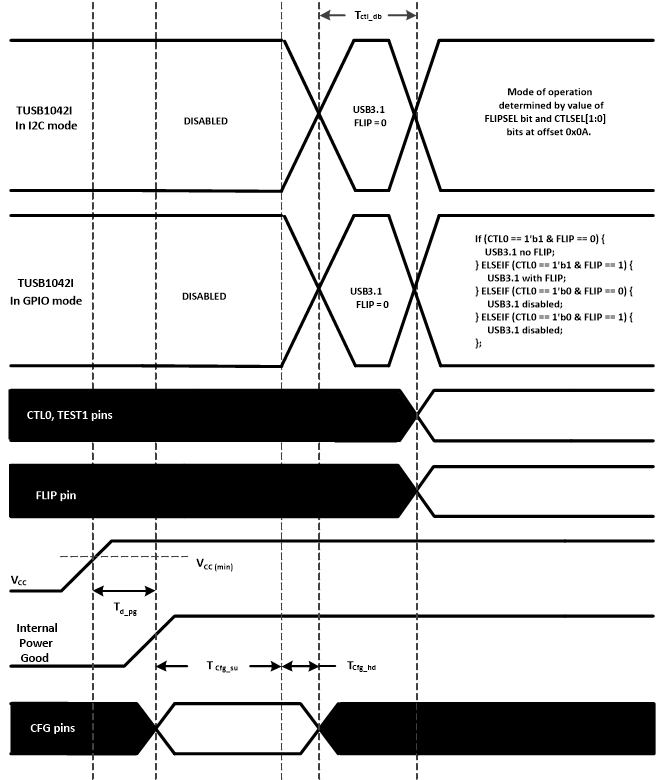
TUSB1042I TUSB1042_Power_Up_Timing_SLLSF15.gifFigure 14. Power-Up Timing

Table 6. Power-Up Timing(1)(2)

PARAMETER MIN MAX UNIT
td_pg VCC (minimum) to Internal Power Good asserted high 500 µs
tcfg_su CFG(1) pins setup(2) 250 µs
tcfg_hd CFG(1) pins hold 10 µs
tCTL_DB TEST1, CTL0 and FLIP pin debounce 16 ms
tVCC_RAMP VCC supply ramp requirement 100 ms
Following pins comprise CFG pins: I2C_EN, EQ[1:0], and SSEQ[1:0].
Recommend CFG pins are stable when VCC is at min.