ZHCSAQ2B January 2013 – April 2017 TS3A5223
PRODUCTION DATA.
8 Detailed Description
8.1 Overview
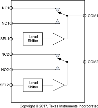
The TS3A5223 is a bidirectional, 2-channel, single-pole double-throw (2:1 SPDT) analog switch that is designed to operate from 1.65 V to 3.6 V. This switch solution comes in a small 1.4mm x 1.8 mm QFN package while maintaining excellent signal integrity, which makes the TS3A5223 suitable for a wide range of applications in personal electronics, portable instrumentation, and test and home electronics. The device maintains the signal integrity by its low ON-state resistance, excellent ON-state resistance matching, and total harmonic distortion (THD) performance. To prevent signal distortion during the transferring of a signal from one channel to another, the TS3A5223 device also has a specified break-before-make feature.
8.2 Functional Block Diagram

8.3 Feature Description
8.3.1 Digital Logic Translation
The TS3A5223 devices supports down to 1-V logic signals irrespective of the supply voltage. The device accomplishes this with integrated level shifters on the digital input SEL1 and SEL2 pis.
8.3.2 Break-Before-Make
The TS3A5223 devices prevents signal distortions when switching signals between the NO and NC pins by completely turning off one signal path before turning on the other signal path. The break-before-make timing specifications are found in the Electrical Characteristics table.
8.4 Device Functional Modes
Logic low voltage on SEL1 or SEL2 pins connect the COM pin to NC pin.
Logic high voltage on SEL1 or SEL2 pins connect the COM pin to NO pin.
Table 1. TS3A5223 Function Table
| SEL1 | SEL2 | COM1 | COM2 |
|---|---|---|---|
| 0 | 0 | NC1 | NC2 |
| 1 | 1 | NO1 | NO2 |
| 1 | 0 | NO1 | NC2 |
| 0 | 1 | NC1 | NO2 |