ZHCSCS9 SEPTEMBER 2014 TPS92661-Q1
PRODUCTION DATA.
- 1 特性
- 2 应用
- 3 说明
- 4 修订历史记录
- 5 Pin Configuration and Functions
- 6 Specifications
-
7 Detailed Description
- 7.1 Overview
- 7.2 Functional Block Diagram
- 7.3
Feature Description
- 7.3.1 Controlling the Internal LED Bypass Switches
- 7.3.2 Internal Switch Resistance
- 7.3.3 PWM Dimming
- 7.3.4 PWM Clock
- 7.3.5 PWM Synchronization
- 7.3.6 Switch Slew Control
- 7.3.7 Effect of Phase Shifting LED Duty Cycles
- 7.3.8 LED Fault Detection and Protection
- 7.3.9 Glitch-Free Operation
- 7.3.10 Internal Oscillator and Watchdog Timers
- 7.4
Device Functional Modes
- 7.4.1
Digital Interface Connections
- 7.4.1.1 Address (ADR0, ADR1, and ADR2 Pins)
- 7.4.1.2 Clock (CLK Pin)
- 7.4.1.3 Internal Charge Pump (CPP Pin)
- 7.4.1.4 Enable (EN Pin)
- 7.4.1.5 GND Pin
- 7.4.1.6 Receive (RX Pin)
- 7.4.1.7 Synchronization (SYNC Pin)
- 7.4.1.8 Transmit (TX Pin)
- 7.4.1.9 Primary Power Supply (VIN Pin)
- 7.4.1.10 On-Board 3.3-V Supply (VCC Pin)
- 7.4.2 Internal Pin-to-Pin Resistance
- 7.4.3 UART Physical Layer
- 7.4.4 UART Clock and Baudrate
- 7.4.5 UART Communications Reset
- 7.4.6 UART Device Addressing
- 7.4.7 UART Communications Protocol
- 7.4.8 Transaction Frame Description
- 7.4.9 Frame Initialization Byte
- 7.4.10 Register Address
- 7.4.11 Data Bytes
- 7.4.12 CRC Bytes
- 7.4.13 Registers
- 7.4.1
Digital Interface Connections
- 7.5 Programming
- 7.6 Register Map
- 8 Application and Implementation
- 9 Power Supply Recommendations
- 10Layout
- 11器件和文档支持
- 12机械封装和可订购信息
8 Application and Implementation
8.1 Applications Information
The TPS92661 is capable of shunting any combination of 12 series LEDs at high frequency and at variable duty cycles. This type of application requires a high bandwidth current source. The TPS92661 was developed using a high-side sensing hysteretic buck current source and it is this type that is recommended to power the LED channels. boost and/or buck-boost inputs may also be used, but makes the implementation more complicated and lower performance.
8.1.1 Guidelines For Current Source
- Operate at a switching frequency at least 250 times the TPS92661 PWM frequency. A switching frequency between 500 times the PWM frequency and 2000 times the PWM frequency is recommended.
- Operate current source in CCM (continuous conduction mode).
- Minimize capacitance on each LED channel (capacitance between LED0 and LED12) to avoid excessive over and undershoot when dimming.
- Monitor the current source output current during dimming to ensure the source is staying close to its DC set-point level.
- Follow the Layout Guidelines.
8.2 Design Examples
This section offers two design examples. Each helps illustrate how the thermal limitations of a design can vary depending on overall operating conditions and how the overall system temperature limitations directly affect the device current rating for a given design. These temperature limitations must be considered on a case-by-case basis.
8.2.1 12 LED, 1.2-A Application
Step 1. LED Board Requirements
Examine the requirements of the LED load board, assuming the worst case condition: LEDs on continuously. This example assumes a worst case metal core PCB temperature of 125°C to adequately protect the LEDs. Calculate the power required to be dissipated by the LED load board alone using Equation 4.
where
- n is the number of LEDs
Step 2. Estimate Device Power Dissipation
Use Figure 1 to estimate the power dissipation in the TPS92661 device. Assuming a 6-MHz clock and a 146-Hz PWM frequency at 125°C, 4.2 mA at a 5.5-V VCC. The power dissipation calculation is shown in Equation 5.
This value is very small compared to the net power required to be dissipated by the LED load and can be neglected.
Step 3. Estimate Switch Power Dissipation
Calculate the worst case power dissipated in the TPS92661 switches. Using the worst case RALL(on) of 3400 mΩ for Equation 6.
Step 4. Calculate the Temperature Rise
The LED load board controls temperature to a maximum of 125°C. Solder the TPS92661 device to the LED board to create a very good thermal connection. Using the TPS92661 θJB measurement of 6.1 °C/W, can calculate the temperature rise between the TPS92661 thermal pad and the junction temperature using Equation 7.
This is the maximum allowable junction temperature. Any time a TPS92661 internal switch is active, the net power dissipated by the LED load board is reduced.
A properly designed LED load board inherently supports the additional power dissipation of the TPS92661 device. In this example, if all of the TPS92661 internal switches are on, the LED load board thermal loading reduces from 44 W to 4.114 W.
8.2.2 6 LED, 1.5-A Application
The TPS92661 can be used for LED loads from 1 to 12 LEDs. When configuring for connections having fewer than 12 LEDs, the LEDs should be connected as shown in Figure 34.
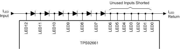 Figure 34. TPS92661 Connection with 6 LEDs
Step 1. Calculate the LED Load Power
As described in the 12 LED, 1.2-A Application section example, the LED load itself drives the heat sink design. Assume the LED load board does not reach a temperature beyond what has been considered for the LEDs. In this case assume the design ensures a maximum heat sink temperature of 90°C for the LED load power calculated in Equation 8.
where
- n is the number of LEDs
Step 2. Estimate the Power Dissipation
Using Figure 3 estimate the power dissipation of the TPS92661 device. Assuming a 8.57-MHz clock and a 523-Hz PWM frequency at 125°C read 3 mA at a 5.5-V VCC. This amount of power is so low that it can be disregarded.
Step 3. Calculate the Worst Case Switches Power Dissipation
Calculate the maximum all switches on-resistance (RALL(on)(MAX)) value for each of the 6 switches that are in use. Assume the other 6 switches are shorted externally.
where
- n is the number of LEDs
Step 4. Calculate the Temperature Rise
The LED load board controls temperature to a maximum of 90°C. Solder the TPS92661 device to the LED board to create a very good thermal connection. Using the TPS92661 θJB measurement of 6.1 °C/W, can calculate the temperature rise between the TPS92661 thermal pad and the junction temperature using
This temperature is well within the TPS92661 operating junction temperature range to provide exceptional performance.