ZHCSCS9 SEPTEMBER 2014 TPS92661-Q1
PRODUCTION DATA.
- 1 特性
- 2 应用
- 3 说明
- 4 修订历史记录
- 5 Pin Configuration and Functions
- 6 Specifications
-
7 Detailed Description
- 7.1 Overview
- 7.2 Functional Block Diagram
- 7.3
Feature Description
- 7.3.1 Controlling the Internal LED Bypass Switches
- 7.3.2 Internal Switch Resistance
- 7.3.3 PWM Dimming
- 7.3.4 PWM Clock
- 7.3.5 PWM Synchronization
- 7.3.6 Switch Slew Control
- 7.3.7 Effect of Phase Shifting LED Duty Cycles
- 7.3.8 LED Fault Detection and Protection
- 7.3.9 Glitch-Free Operation
- 7.3.10 Internal Oscillator and Watchdog Timers
- 7.4
Device Functional Modes
- 7.4.1
Digital Interface Connections
- 7.4.1.1 Address (ADR0, ADR1, and ADR2 Pins)
- 7.4.1.2 Clock (CLK Pin)
- 7.4.1.3 Internal Charge Pump (CPP Pin)
- 7.4.1.4 Enable (EN Pin)
- 7.4.1.5 GND Pin
- 7.4.1.6 Receive (RX Pin)
- 7.4.1.7 Synchronization (SYNC Pin)
- 7.4.1.8 Transmit (TX Pin)
- 7.4.1.9 Primary Power Supply (VIN Pin)
- 7.4.1.10 On-Board 3.3-V Supply (VCC Pin)
- 7.4.2 Internal Pin-to-Pin Resistance
- 7.4.3 UART Physical Layer
- 7.4.4 UART Clock and Baudrate
- 7.4.5 UART Communications Reset
- 7.4.6 UART Device Addressing
- 7.4.7 UART Communications Protocol
- 7.4.8 Transaction Frame Description
- 7.4.9 Frame Initialization Byte
- 7.4.10 Register Address
- 7.4.11 Data Bytes
- 7.4.12 CRC Bytes
- 7.4.13 Registers
- 7.4.1
Digital Interface Connections
- 7.5 Programming
- 7.6 Register Map
- 8 Application and Implementation
- 9 Power Supply Recommendations
- 10Layout
- 11器件和文档支持
- 12机械封装和可订购信息
9 Power Supply Recommendations
9.1 General Recommendations
The TPS92661 requires a 5-V supply to power the charge pump, internal logic and references. This rail generates a 3.3-V supply which can be used for the digital communications as outlined in the Internal Regulator section. The TPS92661 device is not compatible with logic levels lower then 3.3 V or greater than 5 V. A separate, high-power supply drives the LED string, as discussed in the LED Fault Detection and Protection section.
9.2 Internal Regulator
The VCC pin is the output node of the on-board 3.3-V LDO. The VCC pin also acts as the positive voltage rail for the device digital I/Os. If the TPS92661 device is used with a microcontroller with 3.3-V I/Os, then place an output capacitor with a value of at least 0.1 µF at the pin for the internal LDO. Due to the internal linear regulator, an external 3.3-V supply is not required.
If the TPS92661 device is used with 5-V microcontrollers, then the VCC pin MUST be tied to the 5-V VIN pin. This connection overrides the internal LDO and allows the digital I/Os to signal at 5 V rather than 3.3 V.
In the rare case that the digital signaling exists at a voltage greater than 3.6 V, but less than 4.5 V, then the VCC pin should be connected to the same voltage as the MCU I/O voltage.
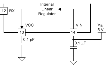 Figure 35. Power Connections for 3.3-V MCU Systems
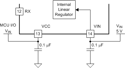 Figure 37. Power Connections for 3.6-V to 4.5-V MCU Systems
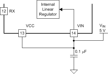 Figure 36. Power Connections for 5-V MCU Systems
9.3 Power Up and Reset
When VIN is greater than VIN-UVT , all bypass switches are initially on (LEDs off) and the LEDs remain off until the device is programmed with the corresponding LED and ENABLE registers. After the registers are programmed, the TPS92661 device modulates the LEDs using the divided-down CLK input as the PWM clock. VIN must be greater than VIN-UVT prior to sourcing current through the LED string in order to ensure a controlled start-up.
The EN input acts as an active-low reset signal for the TPS92661 device. If EN = 0, the TPS92661 device resets to the same state as if a power cycle had occurred. All registers are reset to default values and all of the bypass switches are turned on (LEDs off). Once the device emerges from the reset state by setting EN high, the registers must be programmed in order for the device to begin normal operation.
9.4 VIN Power Consumption
Power consumption increases with increased clock frequency, with VIN voltage and with temperature. It is always best to select the lowest VIN and clock frequency the system can tolerate. Guidelines for power drawn by the device from VIN are provided in the Typical Characteristics section.
9.5 Initialization Set-Up
Figure 38 outlines the steps required to begin communication with a TPS92661 and enable the LEDs. Register Read and Write code examples are shown in the Programming section.
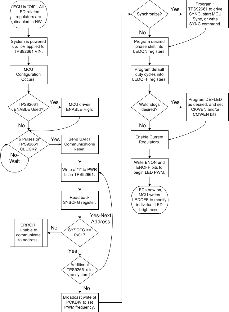 Figure 38. Power Up Sequence