ZHCSCC8E March 2014 – July 2018 TPS92601-Q1 , TPS92602-Q1
UNLESS OTHERWISE NOTED, this document contains PRODUCTION DATA.
- 1 特性
- 2 应用范围
- 3 说明
- 4 修订历史记录
- 5 Pin Configuration and Functions
- 6 Specifications
-
7 Detailed Description
- 7.1 Overview
- 7.2 Functional Block Diagram
- 7.3
Feature Description
- 7.3.1 Fixed-Frequency PWM Control
- 7.3.2 Slope-Compensation Output Current
- 7.3.3 Boost-Current Limit
- 7.3.4 Oscillator and PLL
- 7.3.5 Control Loop Compensation
- 7.3.6 LED Open-Circuit Detection
- 7.3.7 Output Short-Circuit and Overcurrent Detection
- 7.3.8 Measuring LED Current During a Non-Failure Condition
- 7.3.9 LED Dimming Options
- 7.4 Device Functional Modes
-
8 Application and Implementation
- 8.1 Application Information
- 8.2
Typical Applications
- 8.2.1
Boost Regulator With Separate or Paralleled Channels
- 8.2.1.1 Design Requirements
- 8.2.1.2
Detailed Design Procedure
- 8.2.1.2.1 Switching Frequency
- 8.2.1.2.2 Maximum Output-Current Set Point
- 8.2.1.2.3 Output Overvoltage-Protection Set Point
- 8.2.1.2.4 Duty Cycle Estimation
- 8.2.1.2.5 Inductor Selection
- 8.2.1.2.6 Rectifier Diode Selection
- 8.2.1.2.7 Output Capacitor Selection
- 8.2.1.2.8 Input Capacitor Selection
- 8.2.1.2.9 Current Sense and Current Limit
- 8.2.1.2.10 Switching MOSFET Selection
- 8.2.1.2.11 Loop Compensation
- 8.2.1.3 Application Curves
- 8.2.2
Boost-to-Battery Regulator
- 8.2.2.1 Design Requirements
- 8.2.2.2
Detailed Design Procedure
- 8.2.2.2.1 Switching Frequency
- 8.2.2.2.2 Maximum Output-Current Set Point
- 8.2.2.2.3 Output Overvoltage-Protection Set Point
- 8.2.2.2.4 Duty Cycle Estimation
- 8.2.2.2.5 Inductor Selection
- 8.2.2.2.6 Rectifier Diode Selection
- 8.2.2.2.7 Output Capacitor Selection
- 8.2.2.2.8 Input Capacitor Selection
- 8.2.2.2.9 Current Sense and Current Limit
- 8.2.2.2.10 Switching MOSFET Selection
- 8.2.2.2.11 Loop Compensation
- 8.2.2.3 TPS92602y-Q1 Application Curves
- 8.2.1
Boost Regulator With Separate or Paralleled Channels
- 9 Power Supply Recommendations
- 10Layout
- 11器件和文档支持
- 12机械、封装和可订购信息
7.3.5 Control Loop Compensation
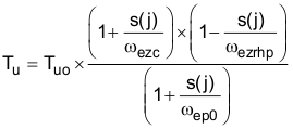
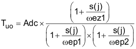
Modeling of the TPS9260xy-Q1 control loop is like that for any current-mode controller. Using a first-order approximation, one can model the uncompensated loop as a single pole created by the output capacitor and, in the boost and buck-boost topologies, a right half-plane zero created by the inductor, where both have a dependence on the dynamic resistance of the LED string. There is also in the model a high-frequency pole which, however, is near the switching frequency and plays no part in the compensation design process. Therefore, the loop analysis neglects this high-frequency pole. Because TI recommends ceramic capacitors for use with LED drivers due to long lifetimes and high ripple-current rating, one can also neglect the ESR of the output capacitor in the loop analysis. Finally, there is a dc gain of the uncompensated loop which depends on internal controller gains and the external sensing network. A boost regulator serves as an example case. See the Detailed Design Procedure section for compensation of all topologies.
Equation 3 gives the whole-loop gain for a boost regulator.

Equation 4 approximates the output pole (ωep0).

where
- r(D): LED and R(ILED_SNS) dynamic resistance
- CO: Output capacitor
Use Equation 5 to calculate the right half-plane zero (ωezrhp).

Use Equation 6 to calculate the output capacitor and ESR zero (ωezc).

The EA transfer function with compensation capacitor and resistor of the system is described in Equation 7 is shown in Equation 7.

where
Use Equation 8 to calculate the EA output with compensation capacitor pole (ωep1).

where
The EA higher frequency pole (ωep2 to filter the high-frequency noise, which is higher than whole-loop bandwidth) is shown in Equation 9.

The EA output ESR zero (ωez1) is shown in Equation 10.

Compensator design should give adequate phase margin (above 45°) at the crossover frequency. A simple compensator using a single capacitor at the COMP pin adds a dominant pole to the system, which ensures adequate phase margin if placed low enough. At high duty cycles, the RHP zero places extreme limits on the achievable bandwidth with this type of compensation. However, because an LED driver is essentially free of output transients (except catastrophic failures, open or short), the dominant pole approach, even with reduced bandwidth, is usually the best approach.