ZHCSCJ5A June 2014 – June 2014 TPS82740A , TPS82740B
PRODUCTION DATA.
- 1 特性
- 2 应用范围
- 3 说明
- 4 典型应用
- 5 修订历史记录
- 6 Device Comparison Table
- 7 Pin Configuration and Functions
- 8 Specifications
- 9 Parameter Measurement Information
- 10Detailed Description
- 11Application and Implementation
- 12Power Supply Recommendations
- 13Layout
- 14器件和文档支持
- 15机械封装和可订购信息
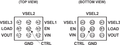
7 Pin Configuration and Functions
MicroSIP™
9 Bump

Table 1. Pin Functions
| PIN | I/O | DESCRIPTION | |
|---|---|---|---|
| NAME | NO | ||
| VIN | C3 | IN | Input voltage supply pin of the module. |
| GND | C2 | - | Ground terminal. |
| CTRL | B2 | IN | CTRL pin controls the LOAD output pin. With CTRL = low, the LOAD output is disabled. This pin must be terminated and not left floating. |
| VOUT | C1 | OUT | Output voltage pin of the module. An internal load switch is connected between VOUT pin and LOAD pin. |
| LOAD | B1 | OUT | Load switch output pin controlled by the CTRL pin. With CTRL = high, an internal load switch connects the LOAD pin to the VOUT pin. The LOAD pin allows connect / disconnect other system components to the output of the DC/DC converter. This pin is pulled to GND with the CTRL pin = low. The LOAD pin features soft switching. If not used, leave the pin open. |
| VSEL3 | A1 | IN | Output voltage selection pins. See Table 2 and Table 3 for VOUT selection. These pins must be terminated and can be changed during operation. |
| VSEL2 | A2 | IN | |
| VSEL1 | A3 | IN | |
| EN | B3 | IN | High level enables the devices and low level turns the device into shutdown mode. This pin must be terminated and not left floating. |
Table 2. Output Voltage Setting TPS82740A
| Device | VOUT | VSEL3 | VSEL2 | VSEL1 |
|---|---|---|---|---|
| TPS82740A | 1.8 | 0 | 0 | 0 |
| 1.9 | 0 | 0 | 1 | |
| 2.0 | 0 | 1 | 0 | |
| 2.1 | 0 | 1 | 1 | |
| 2.2 | 1 | 0 | 0 | |
| 2.3 | 1 | 0 | 1 | |
| 2.4 | 1 | 1 | 0 | |
| 2.5 | 1 | 1 | 1 |
Table 3. Output Voltage Setting TPS82740B
| Device | VOUT | VSEL3 | VSEL2 | VSEL1 |
|---|---|---|---|---|
| TPS82740B | 2.6 | 0 | 0 | 0 |
| 2.7 | 0 | 0 | 1 | |
| 2.8 | 0 | 1 | 0 | |
| 2.9 | 0 | 1 | 1 | |
| 3.0 | 1 | 0 | 0 | |
| 3.1 | 1 | 0 | 1 | |
| 3.2 | 1 | 1 | 0 | |
| 3.3 | 1 | 1 | 1 |