ZHCSCJ5A June   2014  – June 2014 TPS82740A , TPS82740B

PRODUCTION DATA.  

  1. 特性
  2. 应用范围
  3. 说明
  4. 典型应用
  5. 修订历史记录
  6. Device Comparison Table
  7. Pin Configuration and Functions
  8. Specifications
    1. 8.1 Absolute Maximum Ratings
    2. 8.2 Handling Ratings
    3. 8.3 Recommended Operating Conditions
    4. 8.4 Thermal Information
    5. 8.5 Electrical Characteristics
    6. 8.6 Typical Characteristics
  9. Parameter Measurement Information
  10. 10Detailed Description
    1. 10.1 Overview
    2. 10.2 Functional Block Diagram
    3. 10.3 Feature Description
      1. 10.3.1 DCS-Control
      2. 10.3.2 LOAD Switch
      3. 10.3.3 Output Voltage Selection (VSEL1, VSEL2, VSEL3)
      4. 10.3.4 Output Discharge Function (VOUT and LOAD)
      5. 10.3.5 Internal Current Limit
      6. 10.3.6 CTRL / DVS (Dynamic Voltage Scaling TPS62741)
    4. 10.4 Device Functional Modes
      1. 10.4.1 Enable / Shutdown
      2. 10.4.2 Softstart
      3. 10.4.3 POWER GOOD OUTPUT (PG)
      4. 10.4.4 Automatic Transition into 100% Mode
  11. 11Application and Implementation
    1. 11.1 Application Information
    2. 11.2 Typical Application
      1. 11.2.1 Design Requirements
      2. 11.2.2 Detailed Design Procedure
        1. 11.2.2.1 Input Capacitor Selection
          1. 11.2.2.1.1 Input Buffer Capacitor Selection
        2. 11.2.2.2 Output Capacitor Selection
      3. 11.2.3 Application Curves
  12. 12Power Supply Recommendations
  13. 13Layout
    1. 13.1 Layout Guidelines
    2. 13.2 Layout Example
    3. 13.3 Surface Mount Information
  14. 14器件和文档支持
    1. 14.1 文档支持
      1. 14.1.1 相关链接
    2. 14.2 商标
    3. 14.3 静电放电警告
    4. 14.4 术语表
  15. 15机械封装和可订购信息

封装选项

请参考 PDF 数据表获取器件具体的封装图。

机械数据 (封装 | 引脚)
  • SIP|9
散热焊盘机械数据 (封装 | 引脚)
订购信息

13 Layout

13.1 Layout Guidelines

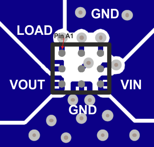
In making the pad size for the uSiP LGA balls, it is recommended that the layout use a non-solder-mask defined (NSMD) land. With this method, the solder mask opening is made larger than the desired land area, and the opening size is defined by the copper pad width. Figure 45 shows the appropriate diameters for a MicroSiPTM layout. Figure 46 shows a suggestion for the PCB layout.

13.2 Layout Example
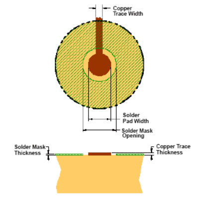
TPS82740A TPS82740B landpad_lvsa57.gifFigure 45. Recommended Land Pattern Image and Dimensions
SOLDER PAD DEFINITIONS(1)(2)(3)(4) COPPER PAD SOLDER MASK (5)
OPENING
COPPER THICKNESS STENCIL (6)
OPENING
STENCIL THICKNESS
Non-solder-mask defined (NSMD) 0.30mm 0.360mm 1oz max (0.032mm) 0.34mm diameter 0.1mm thick
(1) Circuit traces from non-solder-mask defined PWB lands should be 75μm to 100μm wide in the exposed area inside the solder mask opening. Wider trace widths reduce device stand off and affect reliability.
(2) Best reliability results are achieved when the PWB laminate glass transition temperature is above the operating the range of the intended application.
(3) Recommend solder paste is Type 3 or Type 4.
(4) For a PWB using a Ni/Au surface finish, the gold thickness should be less than 0.5mm to avoid a reduction in thermal fatigue performance.
(5) Solder mask thickness should be less than 20 μm on top of the copper circuit pattern.
(6) For best solder stencil performance use laser cut stencils with electro polishing. Chemically etched stencils give inferior solder paste volume control.
TPS82740A TPS82740B TPS82740_PCB_Layout.gifFigure 46. PCB Layout Suggestion

13.3 Surface Mount Information

The TPS82740 MicroSIP™ module uses an open frame construction for a fully automated assembly process and provides a large surface area for pick and place operations. See the "Pick Area" in the package drawing.

Package height and weight have been kept to a minimum, allowing MicroSIP™ device handling similar to a 0805 footprint component.

For reflow recommendations, see document J-STD-20 from the JEDEC/IPC standard.