ZHCSEJ1 December 2015 TPS7H3301-SP
PRODUCTION DATA.
- 1 特性
- 2 应用
- 3 说明
- 4 修订历史记录
- 5 说明 (续)
- 6 Pin Configuration and Functions
- 7 Specifications
- 8 Detailed Description
-
9 Application and Implementation
- 9.1 Application Information
- 9.2
Typical Application
- 9.2.1 Design Requirements
- 9.2.2
Detailed Design Procedure
- 9.2.2.1 VIN/VDD Capacitor
- 9.2.2.2 VLDO Input Capacitor
- 9.2.2.3 VTT Output Capacitor
- 9.2.2.4 VTTSNS Connection
- 9.2.2.5 Low VIN Applications
- 9.2.2.6 S3 and Pseudo-S5 Support
- 9.2.2.7 Tracking Startup and Shutdown
- 9.2.2.8 Output Tolerance Consideration for VTT DIMM Applications
- 9.2.2.9 LDO Design Guidelines
- 9.2.3 Application Curve
- 10Power Supply Recommendations
- 11Layout
- 12器件和文档支持
- 13机械、封装和可订购信息
8 Detailed Description
8.1 Overview
The TPS7H3301-SP device is a sink and source double data rate (DDR) termination regulator specifically designed for low input voltage, low-cost, low-noise systems where space and weight is a key consideration.
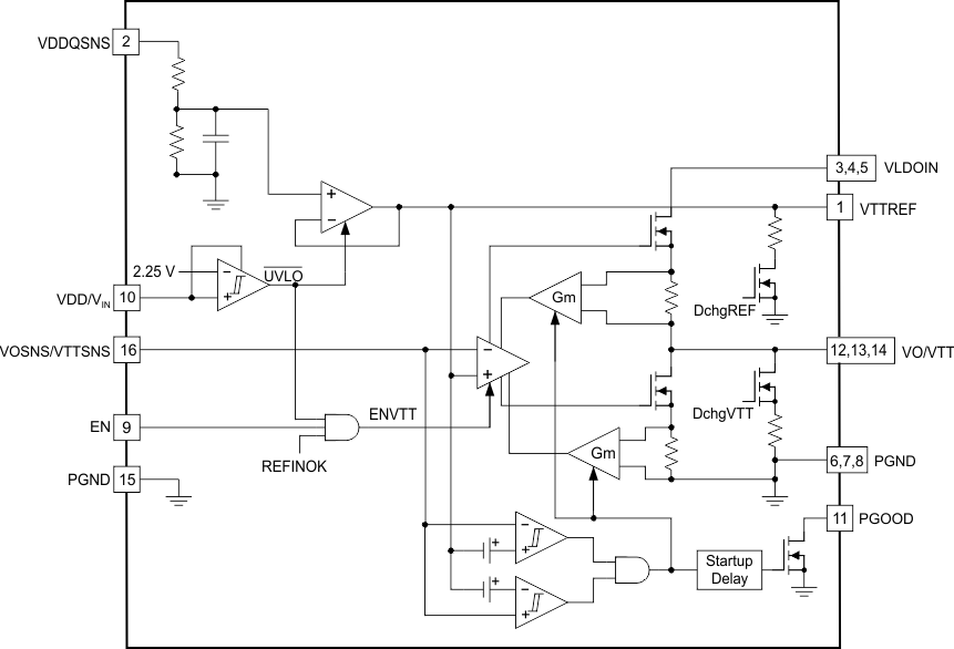
8.2 Functional Block Diagram

8.3 Feature Description
8.3.1 VO Sink/Source Regulator
The TPS7H3301-SP is a 3A sink/source tracking termination regulator specifically designed for low input voltage, low-cost, and low external component count systems where space is a key application parameter. The TPS7H3301-SP integrates a high-performance, low-dropout (LDO) linear regulator that is capable of both sourcing and sinking current. The LDO regulator employs a fast feedback loop so that ceramic capacitors can be used to support the fast load transient response. To achieve tight regulation with minimum effect of trace resistance, a remote sensing pin, VOSNS/VTTSNS, should be connected to the positive pin of the output capacitor(s) as a separate trace from the high current path from Vo/VTT.
The TPS7H3301-SP has a dedicated pin VLDOIN, for VTT power supply to minimize the LDO power dissipation on user application. The minimum VLDOIN voltage is 400mV above the 1/2 VDDQSNS voltage or as highlighted in electrical table VLDOIN to VTT headroom for various load conditions.
8.3.2 Reference Input (VDDQSNS)
The output voltage, Vo/VTT, is regulated to VTTREF. VDDQSNS incorporates integrated resistor divider network. VDDQSNS can be connected to memory supply bus (VDDQ). VDDQSNS should be connected to the memory supply bus (VDDQ). The TPS7H3301-SP supports VDDQSNS voltage from 1.0 V to 3.5 V, making it versatile and ideal for many types of low-power LDO applications.
8.3.3 Reference Output (VTTREF)
When it is configured for DDR termination applications, VTTREF generates the DDR VTT reference voltage for the memory application. VTTREF block consists of an on-chip 1/2 divider and a low-pass filter (LPF). VTTREF tracks 1/2 of VDDQSNS with 1% accuracy. It is capable of supporting both a sourcing and sinking load of 10 mA. VTTREF becomes active when VDDQSNS voltage rises to 0.78 V and Vin/VDD is above the UVLO threshold. When VTTREF is less than 0.375 V, VTTREF is disabled and subsequently discharges to GND through an internal MOSFET. VO/ VTT is also dicharged following discharge of VTTREF. VTTREF is independent of the EN pin state. To meet stability criteria, a capacitor of 0.1 µF min must be installed close to VTTREF (pin1). Capacitor value at VTTREF (pin 1) must not exceed 2.2 µF.
8.3.4 EN ControL (EN)
When EN is driven high, the TPS7H3301-SP Vo/ VTT regulator begins normal operation. When EN is driven low, Vo/VTT is discharges to GND through an internal 18-Ω MOSFET. VTTREF remains on when EN is driven low. EN is not tied high internally to prevent power sequencing issues with an external signal that may be controlling the enable. EN is floating input and not internally tied, thus the user can have complete control over where and when the EN signal is generated. EN feeds directly into PowerGood (PGOOD). When enable is low Pgood is low.
8.3.5 PowerGood Function (PGOOD)
The TPS7H3301-SP provides an open-drain PGOOD output that goes high when the Vo/VTT output is within 20% of VTTREF (typ). PGOOD deasserts within 1 μs after the output exceeds the size of the powergood window. During initial Vo/VTT startup, PGOOD asserts high 2 ms (typ) after the Vo/ VTT enters power good window. Because PGOOD is an open-drain output, a 100-kΩ, pullup resistor between PGOOD and a stable active supply voltage rail is required.
8.3.6 VO Current Protection
The LDO has a constant OCL.
8.3.7 VIN UVLO Protection
For VIN/ VDD undervoltage lockout (UVLO) protection, the TPS7H3301-SP monitors VIN/ VDD voltage. When the VIN/ VDD voltage is lower than the UVLO threshold voltage, both the VTT nd VTTREF regulators are powered off. This shutdown is a non-latch protection.
8.3.8 Thermal Shutdown
The TPS7H3301-SP monitors its junction temperature. If the device junction temperature exceeds its threshold value, (typically 210°C), the VO/VTT and VTTREF regulators are both shut off, discharged by the internal discharge MOSFETs. This shutdown is a non-latch protection.
8.4 Device Functional Modes
TPS7H3301-SP a 3-A source-sink LDO provides low output noise to meet system needs. In order to improve efficiency in the LDO, TPS7H3301-SP LDO can operate from low VLDOIN voltage rail, thus using dual voltage source one for the VLDOIN that supports high current and an alternate voltage source that provides voltage for VDDQSNS pin.
Typcically VLDOIN and VDDQSNS pins are tied together. In the memory system VDDQ is a high-current supply that powers the core, the I/O, and the logic of the memory, VTTREF is a low-current, precision reference voltage that provides a threshold between a logic high (one) and a logic low (zero) that adapts to changes in the I/O supply voltage. By providing a precision threshold that adapts to the supply voltage, VTTREF realizes wider noise margins than those possible with a fixed threshold and normal variations in termination and drive impedance. Specifications vary from device manufacturer to manufacturer, but the most common specification is 0.49 to 0.51 times VDDQ and draws only tens to hundreds of microamps. For TPS7H3301-SP VTTREF is desinged to source / sink 10 mA.