ZHCSIQ1A August   2018  – October 2018 TPS7B70-Q1

PRODUCTION DATA.  

  1. 特性
  2. 应用
  3. 说明
    1.     典型应用
  4. 修订历史记录
  5. Pin Configuration and Functions
    1.     Pin Functions
  6. Specifications
    1. 6.1 Absolute Maximum Ratings
    2. 6.2 ESD Ratings
    3. 6.3 Recommended Operating Conditions
    4. 6.4 Thermal Information
    5. 6.5 Electrical Characteristics
    6. 6.6 Switching Characteristics
    7. 6.7 Typical Characteristics
  7. Detailed Description
    1. 7.1 Overview
    2. 7.2 Functional Block Diagram
    3. 7.3 Feature Description
      1. 7.3.1 Device Enable (EN)
      2. 7.3.2 Adjustable Power-Good Threshold (PG, PGADJ)
      3. 7.3.3 Adjustable Power-Good Delay Timer (DELAY)
      4. 7.3.4 Undervoltage Shutdown
      5. 7.3.5 Current Limit
      6. 7.3.6 Thermal Shutdown
    4. 7.4 Device Functional Modes
      1. 7.4.1 Operation With Input Voltage Less Than 4 V
      2. 7.4.2 Operation With Input Voltage Greater Than 4 V
  8. Application and Implementation
    1. 8.1 Application Information
    2. 8.2 Typical Application
      1. 8.2.1 Design Requirements
      2. 8.2.2 Detailed Design Procedure
        1. 8.2.2.1 Input Capacitor
        2. 8.2.2.2 Output Capacitor
        3. 8.2.2.3 Power-Good Threshold
        4. 8.2.2.4 Power-Good Delay, t(DLY)
      3. 8.2.3 Application Curve
  9. Power Supply Recommendations
  10. 10Layout
    1. 10.1 Layout Guidelines
    2. 10.2 Layout Example
  11. 11器件和文档支持
    1. 11.1 文档支持
      1. 11.1.1 相关文档
    2. 11.2 接收文档更新通知
    3. 11.3 社区资源
    4. 11.4 商标
    5. 11.5 静电放电警告
    6. 11.6 术语表
  12. 12机械、封装和可订购信息

封装选项

机械数据 (封装 | 引脚)
散热焊盘机械数据 (封装 | 引脚)
订购信息

Adjustable Power-Good Threshold (PG, PGADJ)

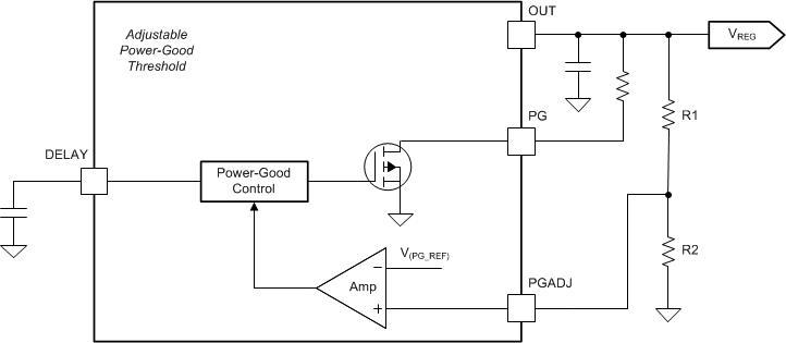
The PG pin is an open-drain output with an external pullup resistor to the regulated supply, and the PGADJ pin is a power-good threshold adjustment pin. Connecting the PGADJ pin to GND sets the power-good threshold value to the default, V(PG_TH). When VOUT exceeds the default power-good threshold, the PG output turns high after the power-good delay has expired. When VOUT falls below V(PG_TH) – V(PG_HYST), the PG output turns low after a short deglitch time.

The power-good threshold is also adjustable from 1.1 V to 5 V by using an external resistor divider between PGADJ and OUT. Equation 1 calculates the threshold:

Equation 1. TPS7B70-Q1 eq01-Vpgadj_SLVSD43.gif

where

  • V(PG_ADJ) is the adjustable power-good threshold
  • V(PG_REF) is the internal comparator reference voltage of the PGADJ pin, 1.1 V typical, 2% accuracy specified under all conditions

By setting the power-good threshold V(PG_ADJ) when VOUT exceeds this threshold, the PG output turns high after the power-good delay has expired. When VOUT falls below V(PG_ADJ) – V(PG_HYST), the PG output turns low after a short deglitch time. Figure 21 shows a block diagram of this threshold.
TPS7B70-Q1 tps7b70-q1-adjustable-power-good-threshold.gifFigure 21. Adjustable Power-Good Threshold