ZHCSBU8D October   2013  – April 2018

PRODUCTION DATA.  

  1. 特性
  2. 应用
  3. 说明
    1.     Device Images
      1.      可调输出选项
      2.      固定输出选项
  4. 修订历史记录
  5. Device Comparison
  6. Pin Configuration and Functions
    1.     Pin Functions
  7. Specifications
    1. 7.1 Absolute Maximum Ratings
    2. 7.2 ESD Ratings
    3. 7.3 Recommended Operating Conditions
    4. 7.4 Thermal Information
    5. 7.5 Electrical Characteristics
    6. 7.6 Timing Requirements
    7. 7.7 Typical Characteristics
  8. Detailed Description
    1. 8.1 Overview
    2. 8.2 Functional Block Diagrams
    3. 8.3 Feature Description
      1. 8.3.1 Enable (EN)
      2. 8.3.2 Regulated Output (VOUT)
      3. 8.3.3 Power-On-Reset (RESET)
      4. 8.3.4 Reset Delay Timer (DELAY)
      5. 8.3.5 Adjustable Output Voltage (ADJ for TPS7B6701)
      6. 8.3.6 Undervoltage Shutdown
      7. 8.3.7 Thermal Shutdown
      8. 8.3.8 Thermal Protection
    4. 8.4 Device Functional Modes
      1. 8.4.1 Operation With VIN < 4 V
      2. 8.4.2 Operation With EN Control
  9. Application and Implementation
    1. 9.1 Application Information
    2. 9.2 Typical Application
      1. 9.2.1 Design Requirements
      2. 9.2.2 Detailed Design Procedure
        1. 9.2.2.1 Power Dissipation and Thermal Considerations
      3. 9.2.3 Application Curves
  10. 10Power Supply Recommendations
    1. 10.1 Dropout Recovery
      1. 10.1.1 LDO Dropout Recovery Explained
      2. 10.1.2 TPS7B67xx-Q1 Dropout During Startup
  11. 11Layout
    1. 11.1 Layout Guidelines
      1. 11.1.1 Enhanced Thermal Pad
      2. 11.1.2 Package Mounting
      3. 11.1.3 Board Layout Recommendations to Improve PSRR and Noise Performance
      4. 11.1.4 Additional Layout Considerations
    2. 11.2 Layout Example
  12. 12器件和文档支持
    1. 12.1 相关链接
    2. 12.2 接收文档更新通知
    3. 12.3 社区资源
    4. 12.4 商标
    5. 12.5 静电放电警告
    6. 12.6 术语表
  13. 13机械、封装和可订购信息

封装选项

机械数据 (封装 | 引脚)
散热焊盘机械数据 (封装 | 引脚)
订购信息

Application Curves

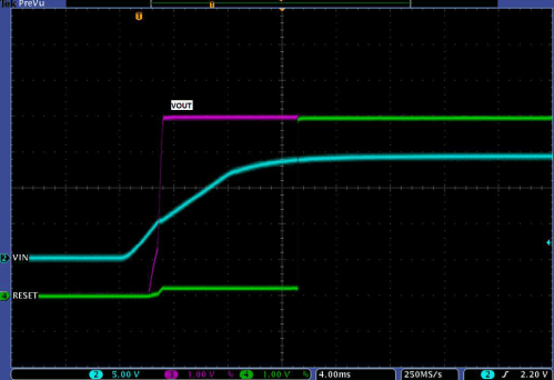
TPS7B6701-Q1 TPS7B6733-Q1 TPS7B6750-Q1 waveform_powerup_slvscb2.gif
Load = 200 mA CIN = COUT = 47 µF
Figure 23. TPS7B6750-Q1 Power-Up Waveform
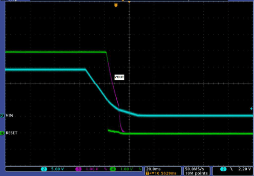
TPS7B6701-Q1 TPS7B6733-Q1 TPS7B6750-Q1 waveform_powerdown_slvscb2.gif
Load = 200 mA CIN = COUT = 47 µF
Figure 24. TPS7B6750-Q1 Power-Down Waveform