ZHCSCE0A April 2014 – April 2014 TPS65980
PRODUCTION DATA.
9 Application and Implementation
9.1 Application Information
The TPS65980 DC/DC switching regulator that receives power from a Thunderbolt™ or Thunderbolt™ 2 power bus ranging from 2.5 V to 15.75 V and generates three separate 3.3-V supply outputs.
9.2 Typical Application
9.2.1 Single-Port Bus-Powered Thunderbolt™ Device
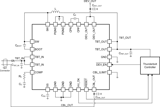 Figure 13. Typical Application (Single-Port Bus-Powered Thunderbolt™ Device)
9.2.1.1 Design Requirements
Table 1. Recommended Component Values
| COMPONENT | DESCRIPTION | MIN | TYP | MAX | UNIT |
|---|---|---|---|---|---|
| CIN | TBT_IN Input Capacitance | 17.6 | 22 | 52 | µF |
| CBOOT | Converter Bootstrap Capacitance | 8 | 10 | 12 | nF |
| CCP | Charge Pump Capacitance (ceramic with ESR ≤ 10 mΩ) | 0.8 | 1 | 1.2 | µF |
| CSS | Soft Start Capacitance | 8 | 10 | 12 | nF |
| CTBT | TBT_OUT Output Capacitance (ceramic with ESR ≤ 10 mΩ) | 16 | 20 | 24 | µF |
| CCBL | CBL_OUT Output Capacitance (ceramic with ESR ≤ 10 mΩ) | 0.8 | 1 | 1.2 | µF |
| CDEV | DEV_OUT Output Capacitance (ceramic with ESR ≤ 10 mΩ) | 0.8 | 1 | 1.2 | µF |
| CC | Compensation Capacitance | 8 | 10 | 12 | nF |
| RC | Compensation Resistance | 8 | 10 | 12 | kΩ |
| L | Inductor SRR1280 (ESR ≤ 20 mΩ) | 8 | 10 | 12 | µH |
9.2.1.2 Detailed Design Procedure
The TPS65980 should use the recommended component values in Table 1. The device is designed to fit the needs of a Thunderbolt™ bus powered peripheral and the recommended component values are chosen to satisfy those conditions. The input capacitance CIN can be as high as 52 µF, but this maximum capacitance must include all capacitances seen at the input to the Thunderbolt™ port.
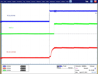
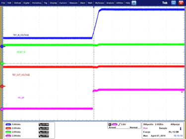
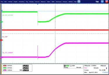
9.2.1.3 Application Performance Plots
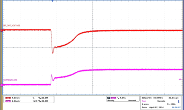
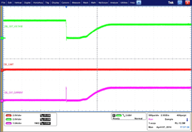
| CTBT_OUT = 10 µF | VTBT_IN = 12 V | |
(0.5A to 3.5A Step)
| CBL_ILIMIT = 0 | ||
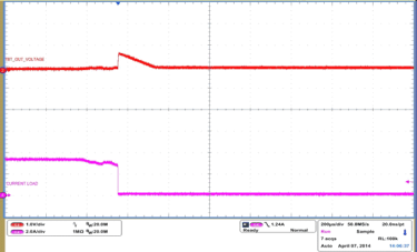
| CTBT_OUT = 10 µF | VTBT_IN = 12 V | |
(3.5A to 0.5A Step)
| CBL_ILIMIT = 1 | ||
9.2.2 Dual-Port Bus-Powered Thunderbolt™ Device
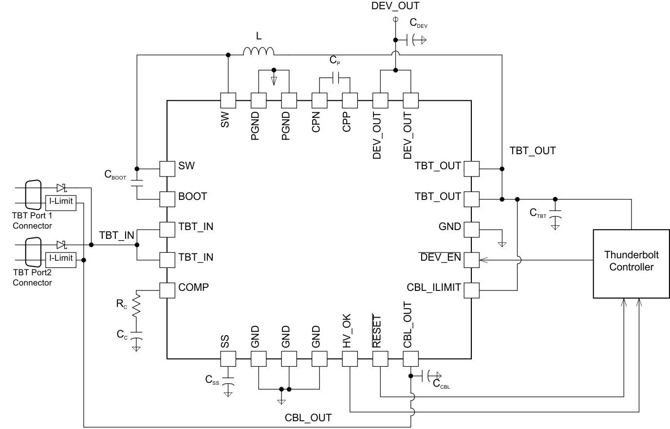 Figure 22. Typical Application (Dual-Port Bus-Powered Thunderbolt™ Device)
9.2.2.1 Design Requirements
In a dual-port application, the TBT_IN input voltage will be selected from either port. A simple diode-or function will produce TBT_IN from the higher of the two inputs. The diode-or selection will allow the high-voltage supply to be at TBT_IN.
In a dual port system, the TPS65980 must provide cable power to both ports. In this case, a second current limiting device (TPS22920) connected between TBT_OUT and the port is recommended. The CBL_OUT pin can also supply current to both ports. In this case, tying CBL_ILIMIT to TBT_OUT will double the amount of current that can be supplied before current limiting. When using this method, the voltage drop to the CBL_OUT pin will increase and care must be taken that other systems resistance do not cause the cable voltage to drop below the allowed pin voltage specified in the Thunderbolt™ specification. To avoid issues with voltage drop in the system, it is recommended that the second port be powered from TBT_OUT as shown in Figure 22. This relieves the voltage drop due to extra current through the CBL_OUT load switch.
Table 2. Recommended Component Values
| COMPONENT | DESCRIPTION | MIN | TYP | MAX | UNIT |
|---|---|---|---|---|---|
| CIN | TBT_IN Input Capacitance | 17.6 | 22 | 52 | µF |
| CBOOT | Converter Bootstrap Capacitance | 8 | 10 | 12 | nF |
| CCP | Charge Pump Capacitance (ceramic with ESR ≤ 10 mΩ) | 0.8 | 1 | 1.2 | µF |
| CSS | Soft Start Capacitance | 8 | 10 | 12 | nF |
| CTBT | TBT_OUT Output Capacitance (ceramic with ESR ≤ 10 mΩ) | 16 | 20 | 24 | µF |
| CCBL | CBL_OUT Output Capacitance (ceramic with ESR ≤ 10 mΩ) | 0.8 | 1 | 1.2 | µF |
| CDEV | DEV_OUT Output Capacitance (ceramic with ESR ≤ 10 mΩ) | 0.8 | 1 | 1.2 | µF |
| CC | Compensation Capacitance | 8 | 10 | 12 | nF |
| RC | Compensation Resistance | 8 | 10 | 12 | kΩ |
| L | Inductor SRR1280 (ESR ≤ 20 mΩ) | 8 | 10 | 12 | µH |
9.2.2.2 Detailed Design Procedure
Refer to Detailed Design Procedure in the Single-Port Bus-Powered Thunderbolt™ Device section.
9.2.2.3 Application Performance Plots
Refer to Application Performance Plots in the Single-Port Bus-Powered Thunderbolt™ Device section.