ZHCSCE0A April 2014 – April 2014 TPS65980
PRODUCTION DATA.
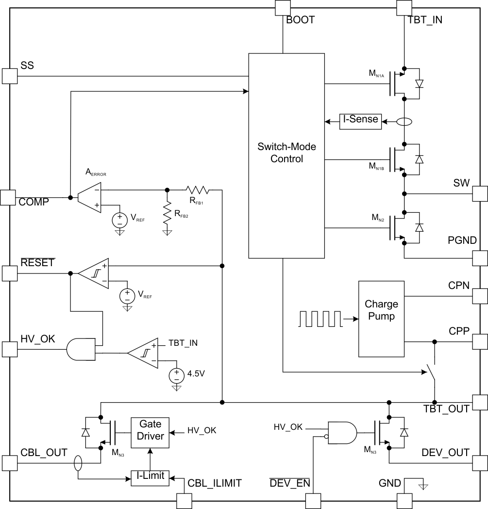
8 Detailed Description
8.1 Overview
The TPS65980 is a switching regulator designed for Thunderbolt™ and Thunderbolt™ 2 bus-powered systems. The TPS65980 receives power from a Thunderbolt™ host in the range of 2.5 V to 15.75 V and produces three separate 3.3 V outputs. TBT_OUT is the main output from the regulator. This output is generated from a switched-cap charge pump when the input is in the low-voltage range. The output is generated from a switching buck converter when the input voltage is in the high-voltage range. The TBT_OUT output powers the local Thunderbolt™ controller and any additional Thunderbolt™ circuitry. Once in the input has settled in the high-voltage range, the other two outputs can be powered from the TBT_OUT output. When the TBT_OUT is supplying 3.3 V, the RESET output asserts high. When the TBT_OUT voltage is below the valid output range, RESET asserts low. When TBT_IN is in the high-voltage input range and RESET is asserting high (valid output), HV_OK will assert high indicating that high-voltage has been received.
The CBL_OUT output supplies power back to the Thunderbolt™ cable for powering the active cable circuitry. This output is connected to the TBT_OUT output with a FET switch and is current limited.
The CBL_ILIMIT logic input pin sets the current limit level. The DEV_OUT output provides power to all other circuitry in the system. This output is not current limited and is enabled/disabled by the DEV_EN logic input.
8.2 Functional Block Diagram
8.3 Feature Description
8.3.1 2.5-V to 15.75-V Input
The TPS65980 is powered from a Thunderbolt™ Bus. This is typically an input to a port from Thunderbolt™ cable. This input will start at 3.3 V (2.5 V ≤ VTBT_IN ≤ 3.4 V) until a link is established between a host and the peripheral device containing the TPS65980. Once the link is established, the voltage at the input can transition to a higher operating voltage (10 V ≤ VTBT_IN ≤ 15.75 V).
8.3.2 3.3-V Outputs
The TPS65980 has three separate 3.3 V outputs. One output, TBT_OUT, is the output from the buck/boost and the other outputs, CBL_OUT and DEV_OUT, are outputs that through load switches from TBT_OUT.
The TBT_OUT supply provides power to the local peripheral Thunderbolt™ controller and support circuitry. The CBL_OUT supply provides power back to the Thunderbolt™ cable and has adjustable current limit. The DEV_OUT supply provides power to all other circuitry in the device to perform its designed function.
8.3.3 Thermal Shutdown
The TPS65980 as a thermal shutdown feature preventing the device from over heating during current limiting situations. The thermal shutdown occurs at a 135°C junction temperature typically. A 10°C hysteresis occurs before the thermal shutdown is cleared.
8.3.4 Cable Power Out Current Limit
The CBL_OUT output is current limited internally. The current limit has two values which are set by the CBL_ILIMIT logic input. When CBL_ILIMIT = 0, the current limit will bet set to 1.1 A typically. When CBL_ILIMIT = 1, the current limit will be set to 2.2 A typically.
8.4 Device Functional Modes
8.4.1 Operation with 2.5 V ≤ VTBT_IN ≤ 3.4 V
The TPS65980 has two normal operating regions. The first region is when 2.5 V ≤ VTBT_IN ≤ 3.4 V. This is the normal power-up state and is termed the low-voltage state. When the input transitions to this range, the input slew rate must meet the SR02L limits. In this voltage range, the TPS65980 operates with a charge pump to generate the nominally 3.3 V output. When the input voltage moves to the higher end of this range, the buck converter takes over to produce the 3.3 V.
8.4.2 Operation with 10 V ≤ VTBT_IN ≤ 15.75 V
In normal operation, the TPS65980 input voltage will transition from the low-voltage range to a high-voltage range where 10 V ≤ VTBT_IN ≤ 15.75 V. This is the high-voltage state and is the state where the TPS65980 will operate most of the time. In this state, the device operates as a buck converter providing a nominally 3.3 V output.