ZHCSCZ1B june 2014 – may 2023 TPS65262-1
PRODUCTION DATA
- 1
- 1 特性
- 2 应用
- 3 说明
- 4 Revision History
- 5 Device Comparison Table
- 6 Pin Configuration and Functions
- 7 Specifications
-
8 Detailed Description
- 8.1 Overview
- 8.2 Functional Block Diagram
- 8.3
Feature Description
- 8.3.1 Adjusting the Output Voltage
- 8.3.2 Enable and Adjusting UVLO
- 8.3.3 Soft-Start Time
- 8.3.4 Power-Up Sequencing
- 8.3.5 V7V Low Dropout Regulator and Bootstrap
- 8.3.6 Out-of-Phase Operation
- 8.3.7 Output Overvoltage Protection (OVP)
- 8.3.8 PSM
- 8.3.9 Slope Compensation
- 8.3.10 Overcurrent Protection (OCP)
- 8.3.11 Power Good
- 8.3.12 Thermal Shutdown
- 8.4 Device Functional Modes
- 9 Application and Implementation
- 10Device and Documentation Support
- 11Mechanical, Packaging, and Orderable Information
8.3.3 Soft-Start Time
The voltage on the SS1 pin controls the start-up of buck1 output. When the voltage on the SS1 pin is less than the internal 0.6-V reference, The TPS65262-1 regulates the internal feedback voltage to the voltage on the SS1 pin instead of 0.6 V, allowing VOUT to rise smoothly from 0 V to its regulated voltage without inrush current. The device has an internal pullup current source of 5 µA (typical) that charges an external soft-start capacitor to provide a linear ramping voltage at SS1 pin.
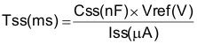
Buck1’s soft-start time can be calculated approximately by Equation 4.
Buck2 and Buck3 have fixed 1-ms soft-start time.
Equation 4.